 80
80
AMD HD 5800 Series Leak Collection Review
Architecture »Specifications
Development in the field of graphics processors relies on technologies that increase realism in 3D graphics applications, and to ensure that the technologies are effectively implemented on the consumers' side, hardware manufacturers develop graphics processors. With each technological milestone, comes a newer more complex graphics processor, and to maintain the complexity while respecting the consumer's implementation budget, companies opt for miniaturization of the graphics processor (GPU). AMD was the first company to come out with a production-grade GPU built on the 40 nm silicon fabrication technology with the RV740 Radeon HD 4700 series. While the GPU itself was flawless, the foundries making it were hit by some snags that reduced the manufacturing output of 40 nm GPUs. As a quick reaction to this, leading GPU manufacturers postured conservative when opting for the new process to build more complex GPUs (since complexity increases size of the GPU, and reduces yields), however, the foundry companies did a good job in overcoming their issues, and 40 nm GPUs, particularly the ATI Radeon HD 4770 have healthy inventories again. Displaying optimism and confidence in its foundry partners, AMD went ahead with developing Cypress, codename for the company's newest, high-performance GPU. Based on this, AMD will be releasing two main GPU SKUs: ATI Radeon HD 5870, and ATI Radeon HD 5850. The two will further be used in variants based on memory size, and special Eyefinity Editions with the necessary connectors for six displays.The numbers in the specifications sheets are mind-boggling. Cypress keeps up with the trend RV770 set, and more than doubles on several of its resources to up the computational power of the GPU.


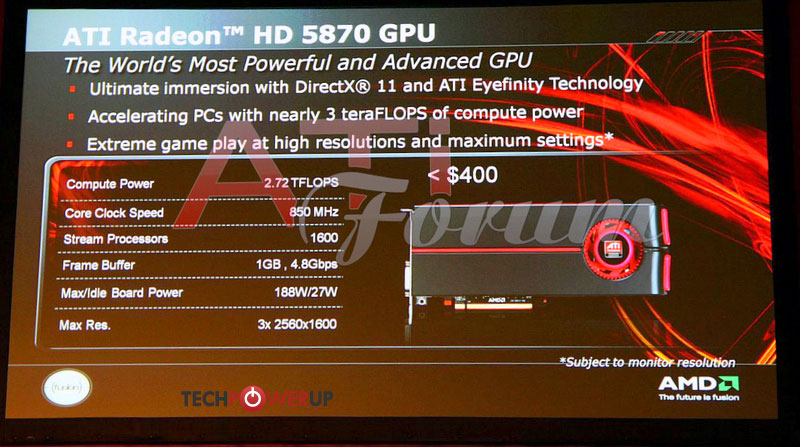
Building a consensus, here's what a Cypress holds in its specs sheet:
- Built on 40 nm fab. process
- Holds 2.15 billion transistors
- Substantially large GPU die going by the standards of 40 nm: 338 mm²
- 1600 stream processors available, all 1600 enabled on Radeon HD 5870, 1440 enabled on Radeon HD 5850
- Shader compute power more than doubled from the previous generation, with Radeon HD 5870 boasting of 2.72 TFLOPs, while Radeon HD 5850 2.08 TFLOPs
- 256-bit GDDR5 memory interface that uses new high-speed, low-latency memory chips. With a memory frequency of 1200 MHz (4.8 GHz effective), Radeon HD 5870 has a memory bandwidth of 153 GB/s, while the memory running at 1000 MHz (4.0 GHz effective) on Radeon HD 5850 churns out 128 GB/s of memory bandwidth
- 80 Texture Memory Units (TMUs), and 32 Raster Opteration (ROP) Units, with Radeon HD 5850 making use of 72 TMUs.
- Full DirectX 11 Shader Model 5.0, and OpenGL 3.2 support
- Support for DirectCompute 11 GPGPU model, and OpenCL
Apr 16th, 2024 02:23 EDT
change timezone
Latest GPU Drivers
New Forum Posts
- Beware: Win11 KB5035853 Cumulative Update may cause stuttering and other performance problems. (13)
- TPU's WCG/BOINC Team (34414)
- Is it possible that the atmosphere is losing less of its "shield" capabilities due to more and more jets/rockets puncturing it daily? (10)
- First time undervolt and benchmark questions (4)
- ASRock Deskmini Owner's Club (23)
- Undervolting Dell XPS 14 9440 is it possible? (4)
- Strange behaviour with my i5 1235u HP laptop after Windows reinstall (6)
- Gigabyte Nvidia 4090 Aorus Master configuration utility other than GCC and OC (3)
- Outer Worlds getting boring (5)
- Which air cooler for a ryzen 9 5900x (130)
Popular Reviews
- Horizon Forbidden West Performance Benchmark Review - 30 GPUs Tested
- PowerColor Radeon RX 7900 GRE Hellhound Review
- Galax GeForce RTX 4070 Super EX Review
- Fractal Design Terra Review
- ASUS GeForce RTX 4090 Matrix Platinum Review - The RTX 4090 Ti
- Corsair 2000D Airflow Review
- Minisforum EliteMini UM780 XTX (AMD Ryzen 7 7840HS) Review
- Creative Pebble X Plus Review
- FiiO KB3 HiFi Mechanical Keyboard Review - Integrated DAC/Amp!
- ASUS GeForce RTX 4090 STRIX OC Review
Controversial News Posts
- NVIDIA Points Intel Raptor Lake CPU Users to Get Help from Intel Amid System Instability Issues (102)
- US Government Wants Nuclear Plants to Offload AI Data Center Expansion (98)
- Developers of Outpost Infinity Siege Recommend Underclocking i9-13900K and i9-14900K for Stability on Machines with RTX 4090 (82)
- Sony PlayStation 5 Pro Specifications Confirmed, Console Arrives Before Holidays (81)
- Windows 10 Security Updates to Cost $61 After 2025, $427 by 2028 (79)
- TechPowerUp Hiring: Reviewers Wanted for Motherboards, Laptops, Gaming Handhelds and Prebuilt Desktops (70)
- Intel Realizes the Only Way to Save x86 is to Democratize it, Reopens x86 IP Licensing (70)
- AMD Zen 5 Execution Engine Leaked, Features True 512-bit FPU (63)