 88
88
ASUS GeForce GTX 570 Review
Test Setup »A Closer Look


The GeForce GTX 570 & 580 are some of the few graphics cards that use a vapor-chamber technology heatplate to maximize heat transfer between the GPU and the rest of the heatsink. You can also see above that the heatsink cools secondary components like voltage regulation circuitry and memory chips. Overall this seems to be a very capable thermal solution but that also increases its price.

Instead of the 6+8 power configuration on the GeForce GTX 580, ASUS has chosen a 6+6 PCI-Express power setup which is sufficient for this card.


In order to stay within the 300 W power limit, NVIDIA has added a power draw limitation system to their GTX 570 and GTX 580. When either Furmark or OCCT are detected running by the driver, three Texas Instruments INA219 sensors measure the inrush current and voltage on all 12 V lines (PCI-E slot, 6-pin, 8-pin) to calculate power. As soon as the power draw exceeds a predefined limit, the card will automatically clock down and restore clocks as soon as the overcurrent situation has gone away. NVIDIA emphasizes this is to avoid damage to cards or motherboards from these stress testing applications and claims that in normal games and applications such an overload will not happen. I am still concerned that with heavy overclocking, especially on water and LN2 the limiter might engage, and reduce clocks which results in reduced performance. Real-time clock monitoring does not show the changed clocks, so besides the loss in performance it could be difficult to detect that state without additional testing equipment or software support.
The second picture shows the jumps in power consumption over time while running Furmark. Compared to the GeForce GTX 580, it seems that the card can now enter several low-frequency states whereas on the GTX 580 it could only reduce the clock speed by 50%.
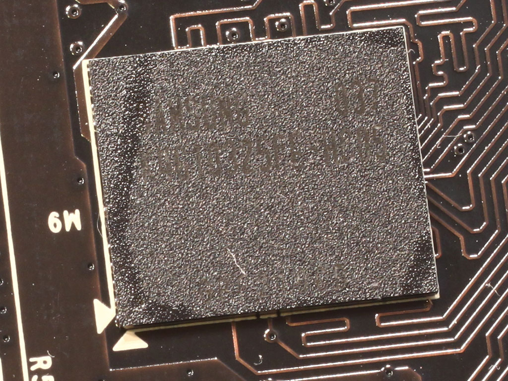
The GDDR5 memory chips are made by Samsung, and carry the model number K4G10325FE-HC04. They are specified to run at 1250 MHz (5000 MHz GDDR5 effective).

Just like on the GeForce GTX 480 and 580, NVIDIA uses a CHiL CHL 8266 voltage regulator on their card. This controller offers extensive monitoring and voltage control options via I2C, so it's a great choice for overclockers.

NVIDIA's GeForce 110 graphics processor is made on a 40 nm process at TSMC Taiwan. It uses approximately 3.0 billion transistors which is 200 million less than the GF100. Please note that the silvery metal surface you see is the heatspreader of the GPU. The actual GPU die is sitting under the heatspreader. According to NVIDIA, the die size of the GF110 graphics processor is 520 mm².
Apr 26th, 2024 12:35 EDT
change timezone
Latest GPU Drivers
New Forum Posts
- 2022-X58/1366 PIN Motherboards NVME M.2 SSD BIOS MOD Collection (657)
- DTS DCH Driver for Realtek HDA [DTS:X APO4 + DTS Interactive] (1909)
- checkup (1)
- Help me to OC my 5700X (10)
- XFX RX470 8GB no video and error 43 (28)
- The TPU UK Clubhouse (24788)
- Secure boot already open help (9)
- im new to throttelstop and i think i messed it up by copying others any hints would be very much aprreciated (4)
- Cs2 Freezing in Rx 580 (5)
- Ghost of Tsushima PC Port !!!! (15)
Popular Reviews
- HYTE THICC Q60 240 mm AIO Review
- MOONDROP x Crinacle DUSK In-Ear Monitors Review - The Last 5%
- Alienware Pro Wireless Gaming Keyboard Review
- Upcoming Hardware Launches 2023 (Updated Feb 2024)
- Thermalright Phantom Spirit 120 EVO Review
- FiiO K19 Desktop DAC/Headphone Amplifier Review
- ASUS Radeon RX 7900 GRE TUF OC Review
- RTX 4090 & 53 Games: Ryzen 7 5800X vs Ryzen 7 5800X3D Review
- NVIDIA RTX 4090: 450 W vs 600 W 12VHPWR - Is there any notable performance difference?
- Sapphire Radeon RX 7900 GRE Pulse Review
Controversial News Posts
- Windows 11 Now Officially Adware as Microsoft Embeds Ads in the Start Menu (127)
- Sony PlayStation 5 Pro Specifications Confirmed, Console Arrives Before Holidays (117)
- NVIDIA Points Intel Raptor Lake CPU Users to Get Help from Intel Amid System Instability Issues (106)
- AMD "Strix Halo" Zen 5 Mobile Processor Pictured: Chiplet-based, Uses 256-bit LPDDR5X (102)
- US Government Wants Nuclear Plants to Offload AI Data Center Expansion (98)
- AMD's RDNA 4 GPUs Could Stick with 18 Gbps GDDR6 Memory (92)
- Developers of Outpost Infinity Siege Recommend Underclocking i9-13900K and i9-14900K for Stability on Machines with RTX 4090 (85)
- Windows 10 Security Updates to Cost $61 After 2025, $427 by 2028 (84)