 25
25
ASUS GeForce GTX 580 1.5 GB Review
Test Setup »A Closer Look
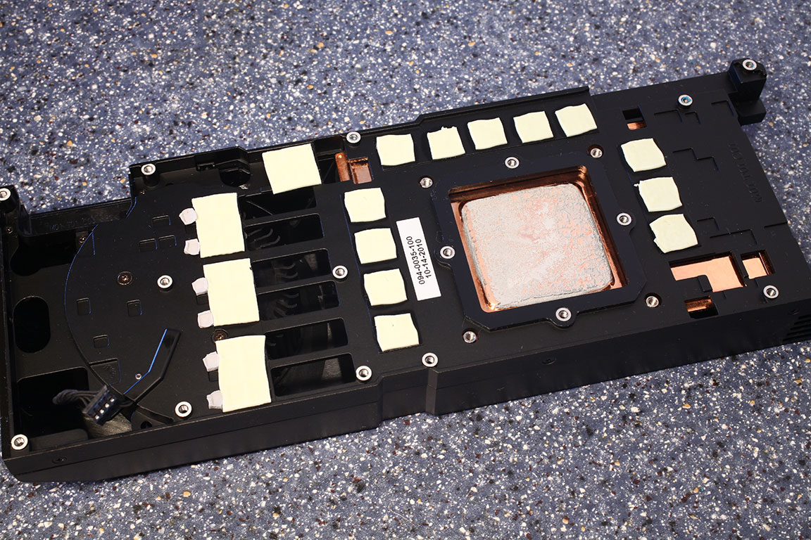
The GeForce GTX 580 is one of the few graphics cards that uses a vapor-chamber technology heatplate to maximize heat transfer between the GPU and the rest of the heatsink. You can also see above that the heatsink cools secondary components like voltage regulation circuitry and memory chips. Overall this seems to be a very capable thermal solution but that also increases its price.

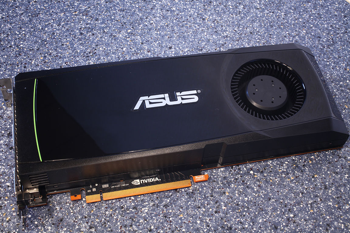
NVIDIA's 6+8 power input configuration is sufficient for the GTX 580 design and provides up to 300 W.
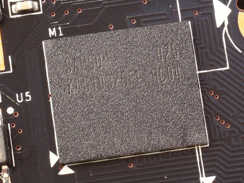
The GDDR5 memory chips are made by Samsung, and carry the model number K4G10325FE-HC04. They are specified to run at 1250 MHz (5000 MHz GDDR5 effective).
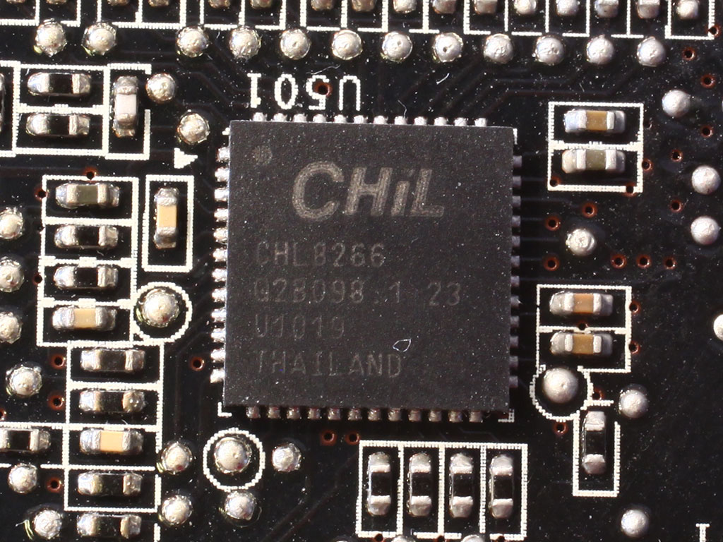
Just like on the GeForce GTX 480, NVIDIA uses a CHiL CHL 8266 voltage regulator on their card. This controller offers extensive monitoring and voltage control options via I2C, so it's a great choice for overclockers.
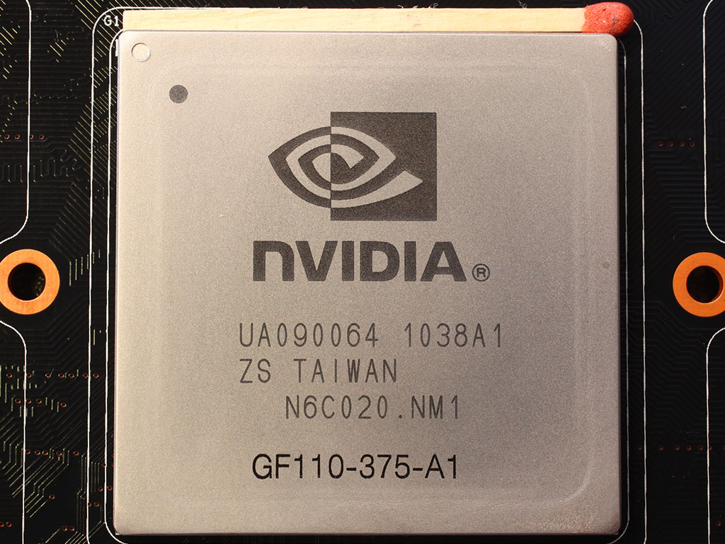
NVIDIA's GeForce 110 graphics processor is made on a 40 nm process at TSMC Taiwan. It uses approximately 3.0 billion transistors which is 200 million less than the GF100. Please note that the silvery metal surface you see is the heatspreader of the GPU. The actual GPU die is sitting under the heatspreader, its dimensions are not known. According to NVIDIA, the die size of the GF110 graphics processor is 520 mm².
Apr 26th, 2024 11:34 EDT
change timezone
Latest GPU Drivers
New Forum Posts
- im new to throttelstop and i think i messed it up by copying others any hints would be very much aprreciated (4)
- The TPU UK Clubhouse (24787)
- Cs2 Freezing in Rx 580 (5)
- Ghost of Tsushima PC Port !!!! (15)
- The Official Linux/Unix Desktop Screenshots Megathread (699)
- Red Dead Redemption using emu (4)
- Meta Horizon OS (21)
- Old high quality PSU, or semi-old mid-quality PSU? (3)
- Secure boot already open help (8)
- What are you playing? (20540)
Popular Reviews
- HYTE THICC Q60 240 mm AIO Review
- MOONDROP x Crinacle DUSK In-Ear Monitors Review - The Last 5%
- Alienware Pro Wireless Gaming Keyboard Review
- Upcoming Hardware Launches 2023 (Updated Feb 2024)
- Thermalright Phantom Spirit 120 EVO Review
- ASUS Radeon RX 7900 GRE TUF OC Review
- FiiO K19 Desktop DAC/Headphone Amplifier Review
- RTX 4090 & 53 Games: Ryzen 7 5800X vs Ryzen 7 5800X3D Review
- NVIDIA RTX 4090: 450 W vs 600 W 12VHPWR - Is there any notable performance difference?
- RTX 4090 & 53 Games: Core i9-13900K vs Ryzen 7 5800X3D Review
Controversial News Posts
- Windows 11 Now Officially Adware as Microsoft Embeds Ads in the Start Menu (125)
- Sony PlayStation 5 Pro Specifications Confirmed, Console Arrives Before Holidays (117)
- NVIDIA Points Intel Raptor Lake CPU Users to Get Help from Intel Amid System Instability Issues (106)
- AMD "Strix Halo" Zen 5 Mobile Processor Pictured: Chiplet-based, Uses 256-bit LPDDR5X (101)
- US Government Wants Nuclear Plants to Offload AI Data Center Expansion (98)
- AMD's RDNA 4 GPUs Could Stick with 18 Gbps GDDR6 Memory (92)
- Developers of Outpost Infinity Siege Recommend Underclocking i9-13900K and i9-14900K for Stability on Machines with RTX 4090 (85)
- Windows 10 Security Updates to Cost $61 After 2025, $427 by 2028 (84)