 28
28
ASUS Maximus IV Gene-Z LGA1155 Review
BIOS Walkthrough »The Board - A Closer Look


The ASUS Maximus IV Gene-Z comes equipped with a 64Mb BIOS chip to hold its customized UEFI firmware. The firmware interacts with the Digi+/EPU VRM controller, which, paired with the "TPU" chip, makes up ASUS's "Dual Intelligent Processor" VRM solution that is found on nearly every enthusiast product ASUS sells. Yes, that is not a typo; there really is a chip labeled "TPU" on the majority of ASUS products today, the very same acronym we use here on the TechPowerUp website, however, in this instance, the letters stand for "Turbo Processing Unit". Or does it? ;)


The VRM itself features a standard Hi/Low MOSFET design, with the six small black square input drivers seen between the MOSFETs, each powering two full phases. With eight phases for the CPU, and four for the GPU, it's easy to spot which phases are which, considering the inductor arrangement. The DIMM VRM is a true dual phase design, as you can see by the second image above, with two sets of Hi/Low MOSFETs, as well as dual inductors, marked "1R2".
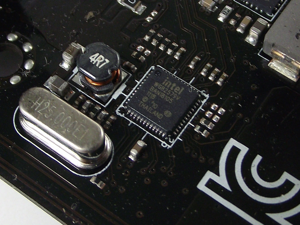
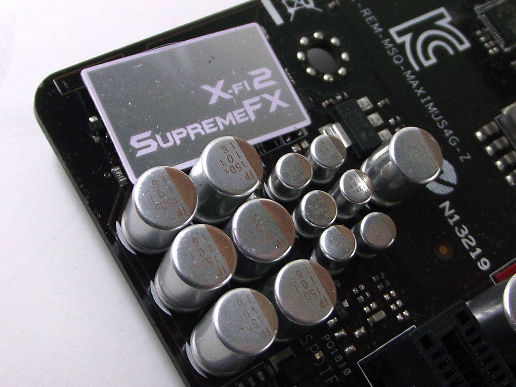
Intel provides the LAN chip, with a highly popular Intel WG82579V PCIe Ethernet controller that claims to use very little CPU time, something that can be critical for maximizing online game performance. For audio, the ASUS Maximus IV Gene-Z features a software-based X-Fi solution that ASUS refers to as the X-Fi 2 SupremeFX, which utilizes a Realtek ALC889 audio CODEC underneath the metal vanity plate shown in the second picture.


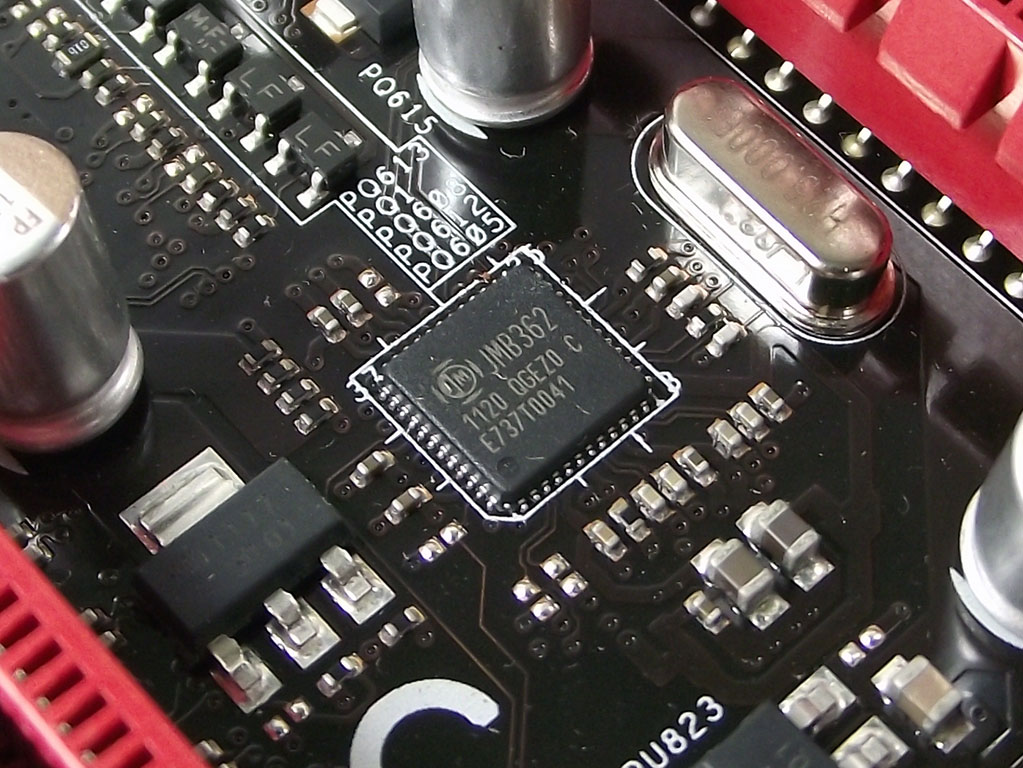
We find as a Super I/O, what has become a common item on ASUS boards, the Nuvoton NCT6776F. The Nuvoton chip is paired up with the iROG chip seen in the second image to provide full voltage and temperature monitoring, as well as fan speed control. To support the eSATA ports we find on the rear I/O, ASUS has employed the JMicron JMB362, an affordable PCIe SATA 3 Gb/s controller we've seen on countless products.

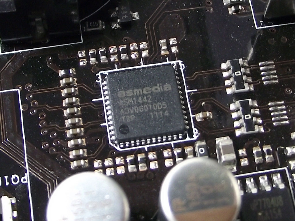


The next several components are provided by AsMedia, starting with the ASM1440 PCIe 2.0 switches that swap lanes from the first PCIe x16 slot to the secondary slot. The second component, the ASM1442, is a TMDS that provides the functionality and voltage shifting needed to support the HDMI port on the rear I/O. The last two AsMedia components are ASM1042 USB 3.0 controllers that ride along the PCIe bus. The first USB 3.0 controller, located just below the DIMM slots and shown in the third image above, provides support for the red USB 3.0 front panel header, while the next image shows the secondary controller, at the rear of the board between the VRM cooler and the rear I/O tower that holds the ports the controller is connected to.


Like the majority of ROG products, ASUS has outfitted the Maximus IV Gene-Z with several buttons; an ON/OFF and a RESET button are found on the board's edge, and they light up when the board is supplied with power, while a third, labeled "GO_BUTTON", provides two distinctly different features. First, it serves to enable ASUS's own "MemOK" functionality, an extra bit of BIOS programming that when the button is pushed before POST is enabled, will test the installed memory and then apply settings it found to be good to guarantee a "safe boot". We've tested this functionality with a set of DIMMs that we know are problematic with most 1155 socket boards, and the "MemOK" function got us into the BIOS, at least, which is more than many other products can claim. Secondly, the "GO_BUTTON" also serves to load-on-the-fly a preset overclock that can be manually configured in the board's BIOS. There is also a set of read points for critical system voltages as we've seen before on other overclocker-friendly products, but these are not our favorite solution, as they are just solder points, and not sockets, which could potentially lead to shorting issues if users are not extremely careful.


For cooling, we find an "L"-shaped cooler for the VRM, composed of two matching aluminum elements with many thick fins, and each element is connected together via a large flattened heatpipe. The multiple fins are shaped to provide a large surface area for cooling, which allows the cooler to do a good job, even when in low air-flow environments. The PCH cooler seems to be composed of a large solid block of aluminum, with the underside milled out a bit so it doesn't contact other components. After flipping both over we find that both make excellent contact with all necessary surfaces, with the VRM cooler showing such deep impressions from the MOSFETs and input drivers that we can see through the pad in places. The PCH cooler uses the common, but adequate bubble-gum thermal interface we've seen many times over now, which through our testing does a fantastic job. It's worth noting that because of how the pad on the VRM cooler appears, we suggest that users do not remove this cooler unless they plan to replace it with a completely different cooler, such as a waterblock, as we do question the effectiveness of the compressed thermal pad once the cooler has been removed.
Apr 26th, 2024 09:38 EDT
change timezone
Latest GPU Drivers
New Forum Posts
- Alphacool CORE 1 CPU block - bulging with danger of splitting? (25)
- Secure boot already open help (4)
- What are you playing? (20539)
- What's your latest tech purchase? (20351)
- The Official Linux/Unix Desktop Screenshots Megathread (698)
- Horizontal black lines popping up on my screen? (12)
- Which new games will you be buying? (321)
- GoDeal24 Windows 11 Pro 32-bit! (3)
- Old high quality PSU, or semi-old mid-quality PSU? (1)
- Best SSD for system drive (86)
Popular Reviews
- HYTE THICC Q60 240 mm AIO Review
- MOONDROP x Crinacle DUSK In-Ear Monitors Review - The Last 5%
- Alienware Pro Wireless Gaming Keyboard Review
- Upcoming Hardware Launches 2023 (Updated Feb 2024)
- Thermalright Phantom Spirit 120 EVO Review
- ASUS Radeon RX 7900 GRE TUF OC Review
- FiiO K19 Desktop DAC/Headphone Amplifier Review
- NVIDIA RTX 4090: 450 W vs 600 W 12VHPWR - Is there any notable performance difference?
- RTX 4090 & 53 Games: Ryzen 7 5800X vs Ryzen 7 5800X3D Review
- RTX 4090 & 53 Games: Core i9-13900K vs Ryzen 7 5800X3D Review
Controversial News Posts
- Windows 11 Now Officially Adware as Microsoft Embeds Ads in the Start Menu (123)
- Sony PlayStation 5 Pro Specifications Confirmed, Console Arrives Before Holidays (117)
- NVIDIA Points Intel Raptor Lake CPU Users to Get Help from Intel Amid System Instability Issues (106)
- AMD "Strix Halo" Zen 5 Mobile Processor Pictured: Chiplet-based, Uses 256-bit LPDDR5X (101)
- US Government Wants Nuclear Plants to Offload AI Data Center Expansion (98)
- AMD's RDNA 4 GPUs Could Stick with 18 Gbps GDDR6 Memory (89)
- Developers of Outpost Infinity Siege Recommend Underclocking i9-13900K and i9-14900K for Stability on Machines with RTX 4090 (85)
- Windows 10 Security Updates to Cost $61 After 2025, $427 by 2028 (84)