 27
27
ASUS Maximus V Formula/ThunderFX Intel LGA 1155 Review
BIOS Walkthrough »The Board - A Closer Look

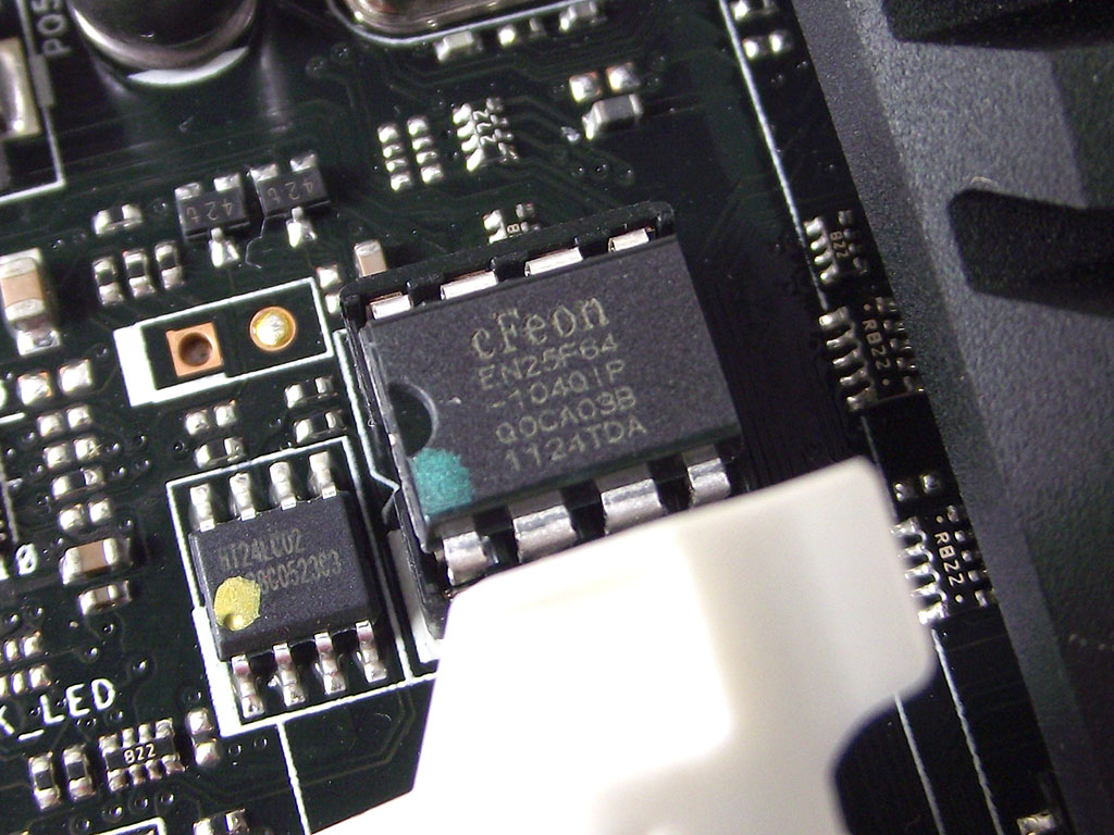
Like most other ASUS ROG products, the Maximus V Formula comes equipped with several buttons that serve well in test-bench installations for benchmarking, or preliminary testing when first assembling a system. All needed functionality, including CMOS Clearing, RESET, ON/OFF, and a few other options, are available before you boot up the board. One of the main ASUS-specific features is a "GO Button" provided to automatically test installed memory and set it to usable settings to ensure boot; a great feature for overclocking memory or for those using older DIMMs. The "GO_Button" also has another use, but we'll talk about that in a minute. Of course, once you power up, the BIOS takes control. The BIOS chip itself resides inside of a user-serviceable socket should you ever need to replace it. That need has greatly dwindled thanks to many other technologies here, but it's definitely nice to have such an option.
ASUS has, of course, fit the Maximus V formula with several other overclocking-centric features, including a set of read points that, combined with a multimeter, can provide real-time voltage monitoring of all critical areas without having to use some form of software. Just to the left of the read points are four LEDs that will light up as the POST process runs. LEDs which remain lit, should the boot fail, point the general area at fault here.
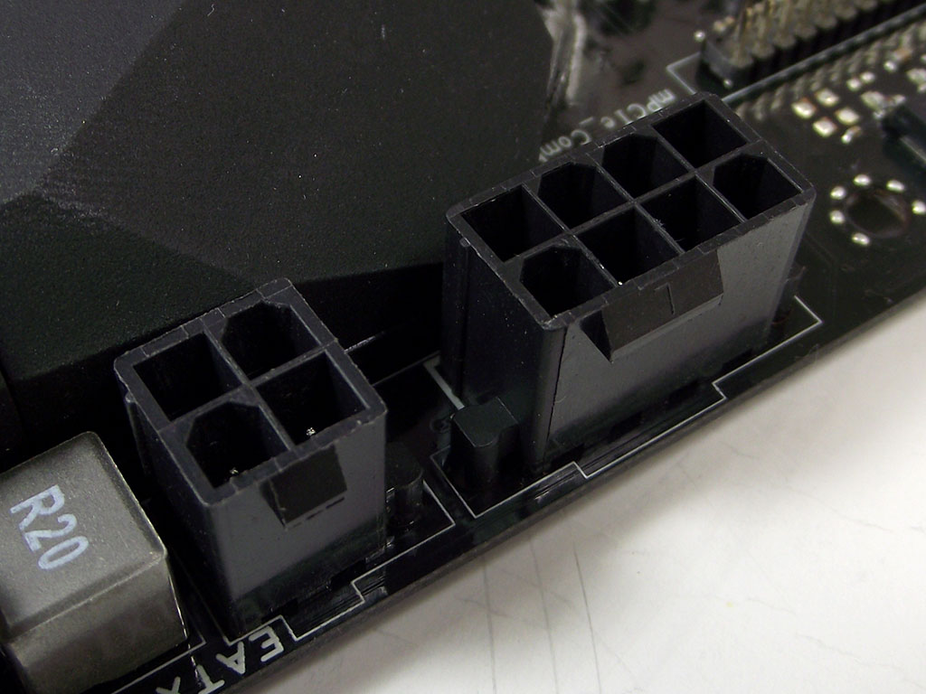

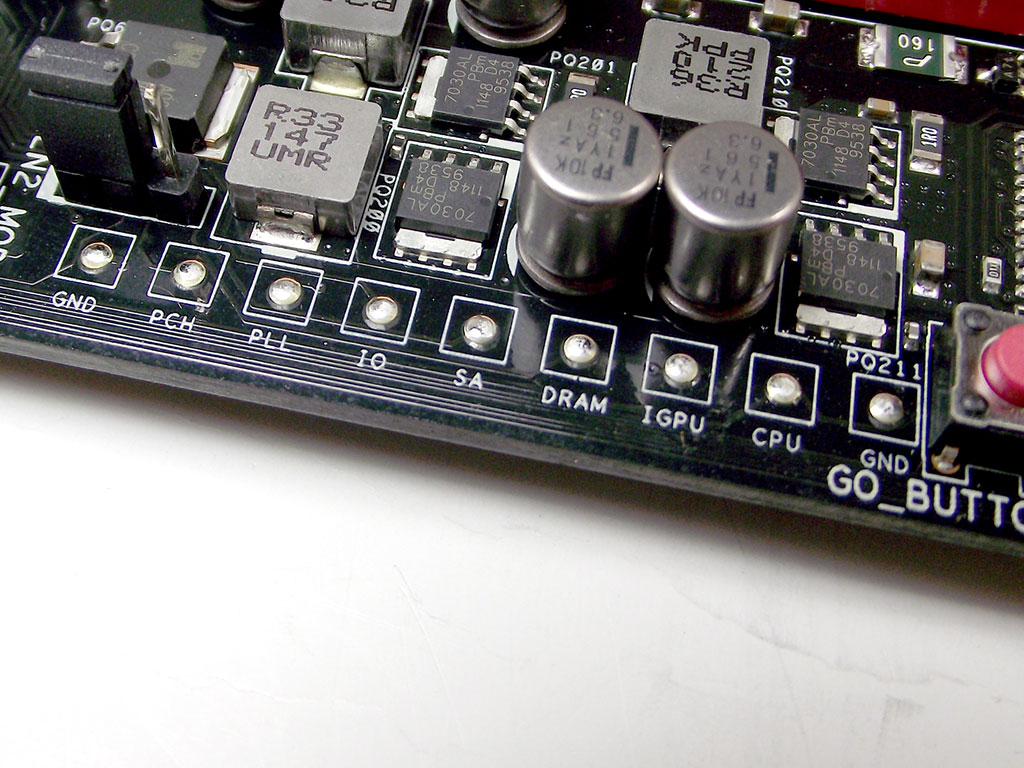
You might think that's more than is needed, but ASUS has added a couple more features, including the addition of a secondary 4-pin EPS power connector that can, optionally, provide the CPU with more power than a 8-pin connecter stand-alone is capable of. There is also a two-position switch labeled "SLOW_MODE", which forces a low CPU multiplier to aid in BCLK and memory overclocking. Next to the SLOW_MODE switch is a dual-digit POST LED display telling you exactly where boot has failed, or if it has succeeded.
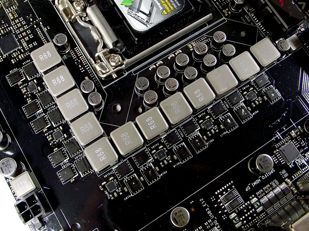

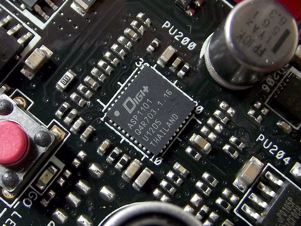
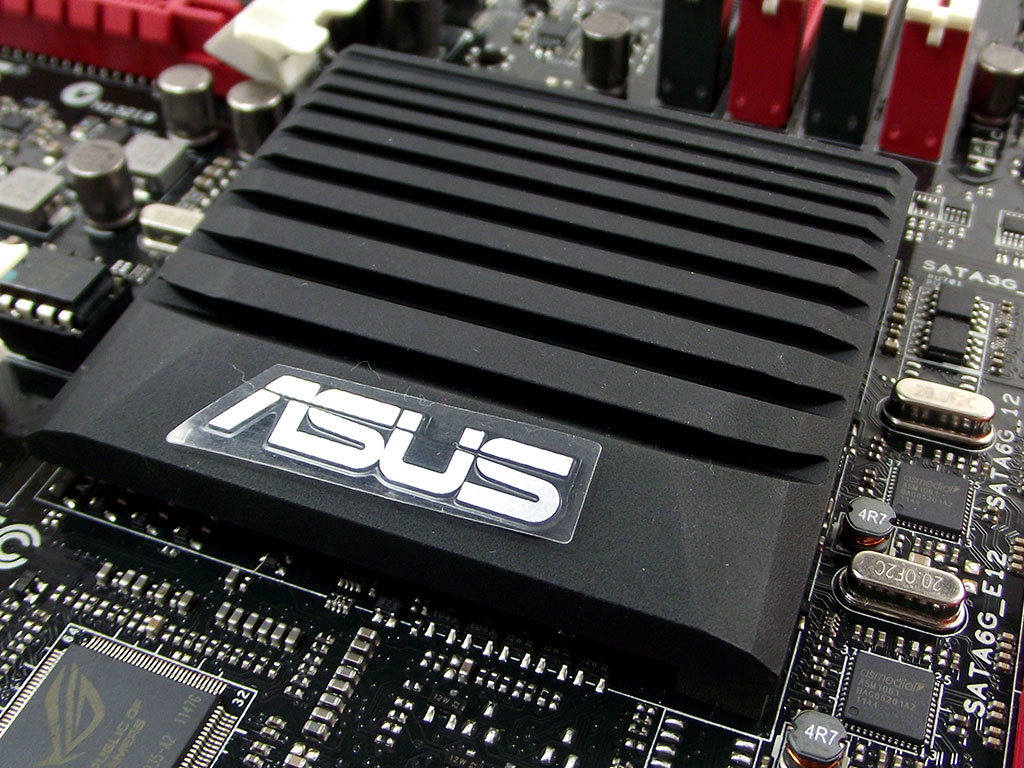
CPU VRM control is provided by a self-branded ASUS DIGI+ controller, pictured above. It controls the 8+4 CPU phases, eight of which are for the CPU proper, with the remaining four for the iGPU portion of the chip. That is a lot more potential power for the iGPU than what some other board makers provide. There are several VRM components mounted to the backside of the board, underneath a very large piece of metal that should act as a heatsink, in order to fit everything in the small space around the socket. This bit of aluminum is overly large, just like the cooler on the front side.
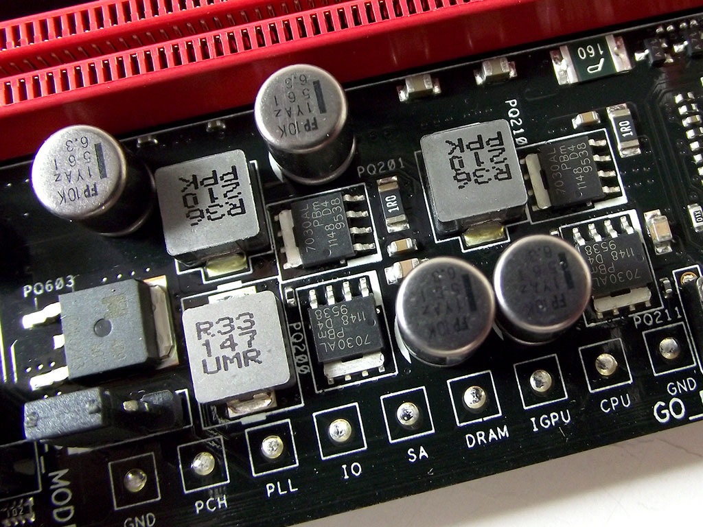

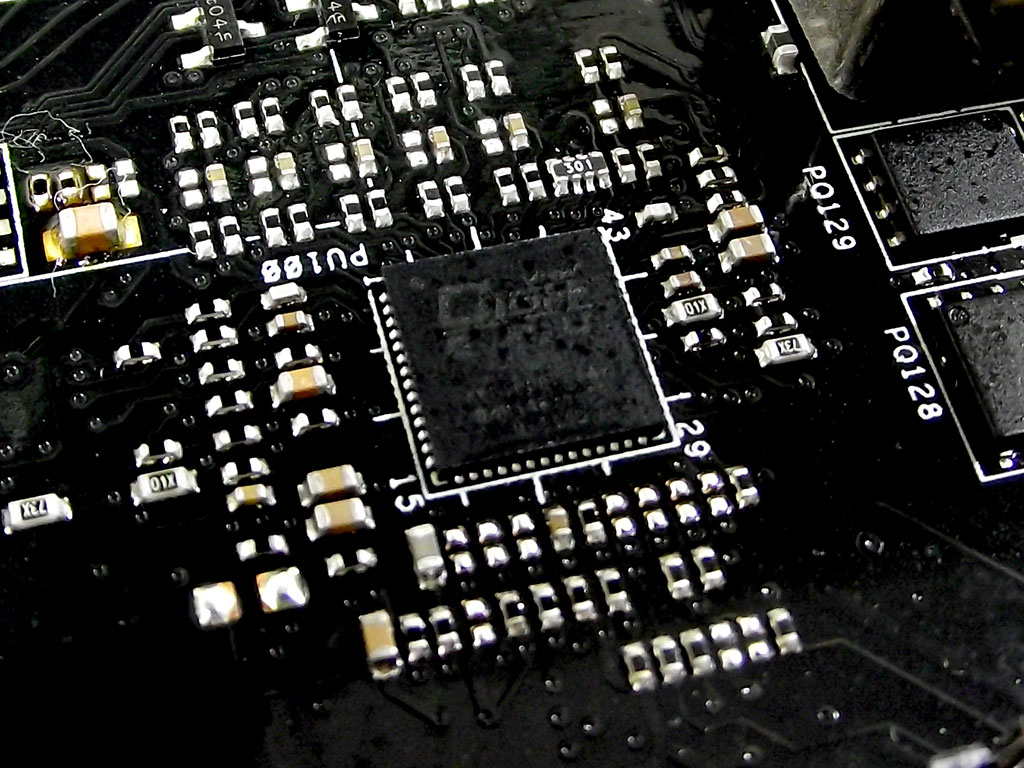
The DIMM VRM is also controlled by a similar DIGI+ controller, but it does seem to be a different model of chip. The VRM itself is dual-phase, and should allow for 3000+ MHz memory speeds when pushing extreme clocks. I found the input drivers on the rear of the board, just below the main VRM components, so some care must be taken when installing the board into a case.
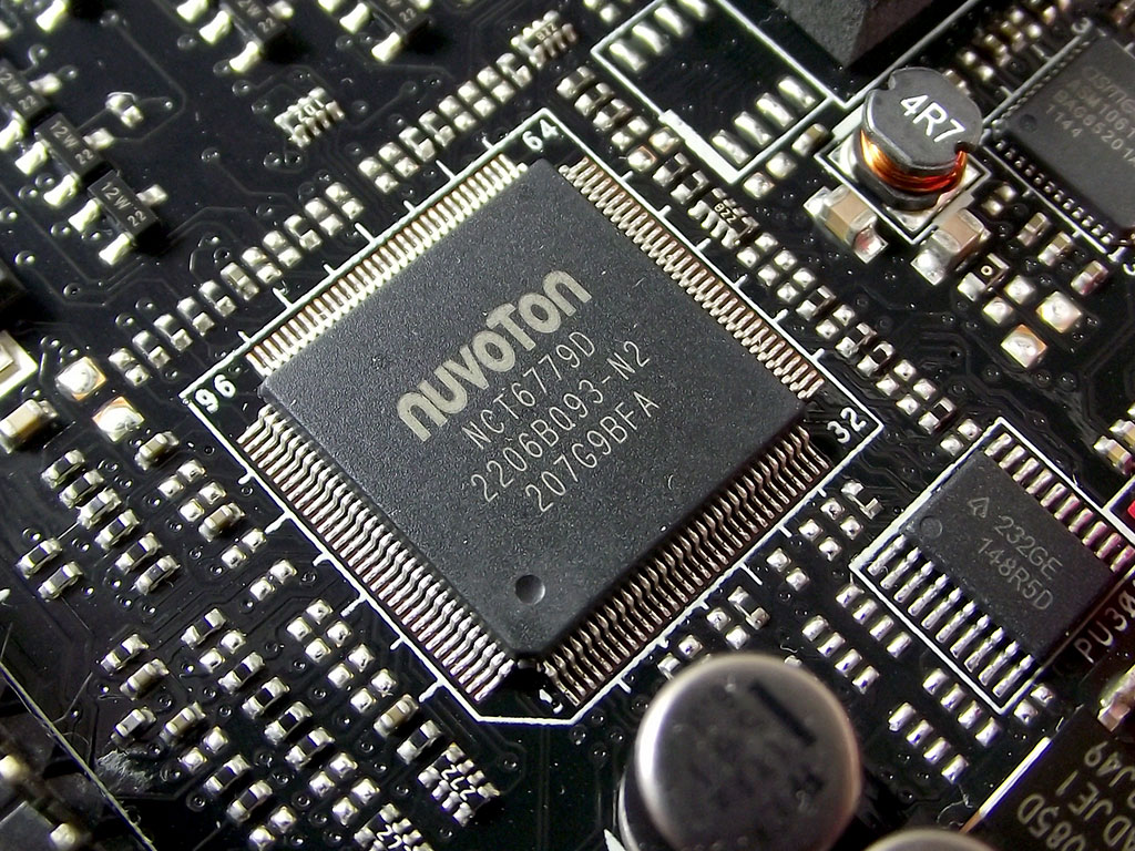

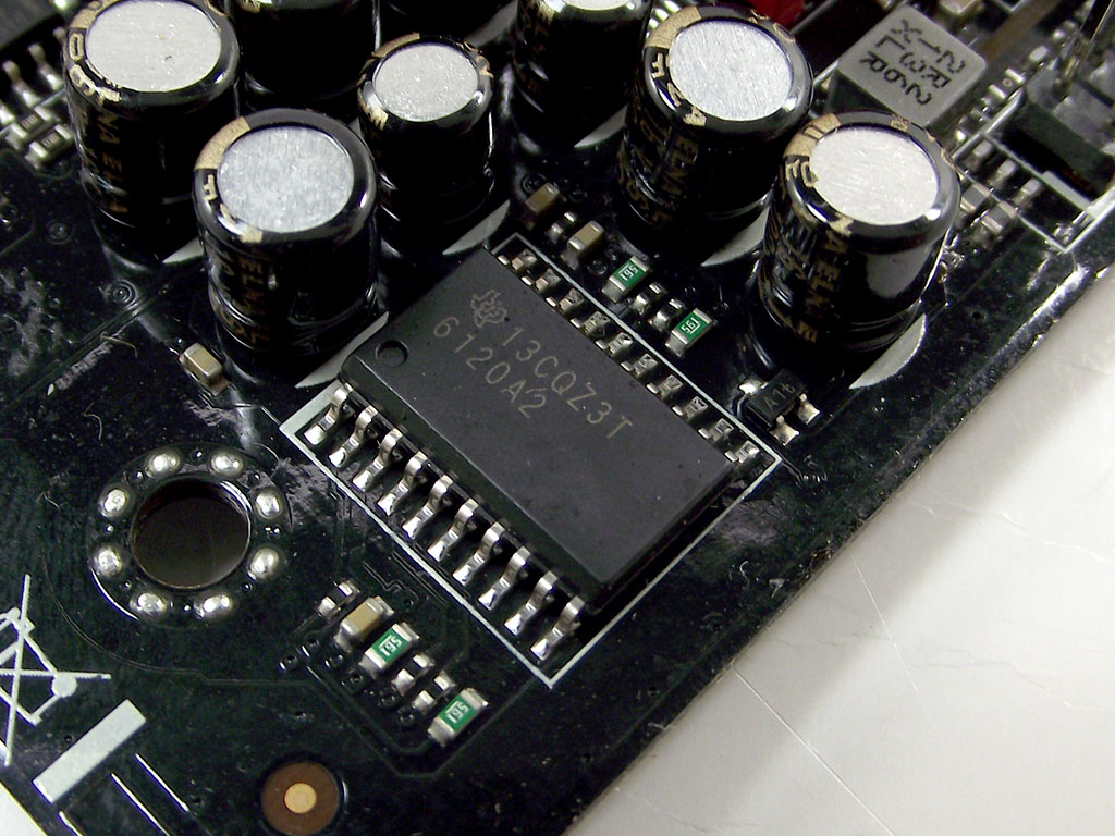
Voltage monitoring, fan control, and such functionality are provided by a pair of chips, one of which is a fairly standard Nuvoton part, while the other is an ROG labeled part. Both chips have very similar physical appearances with even the SMD layout around them being the same.
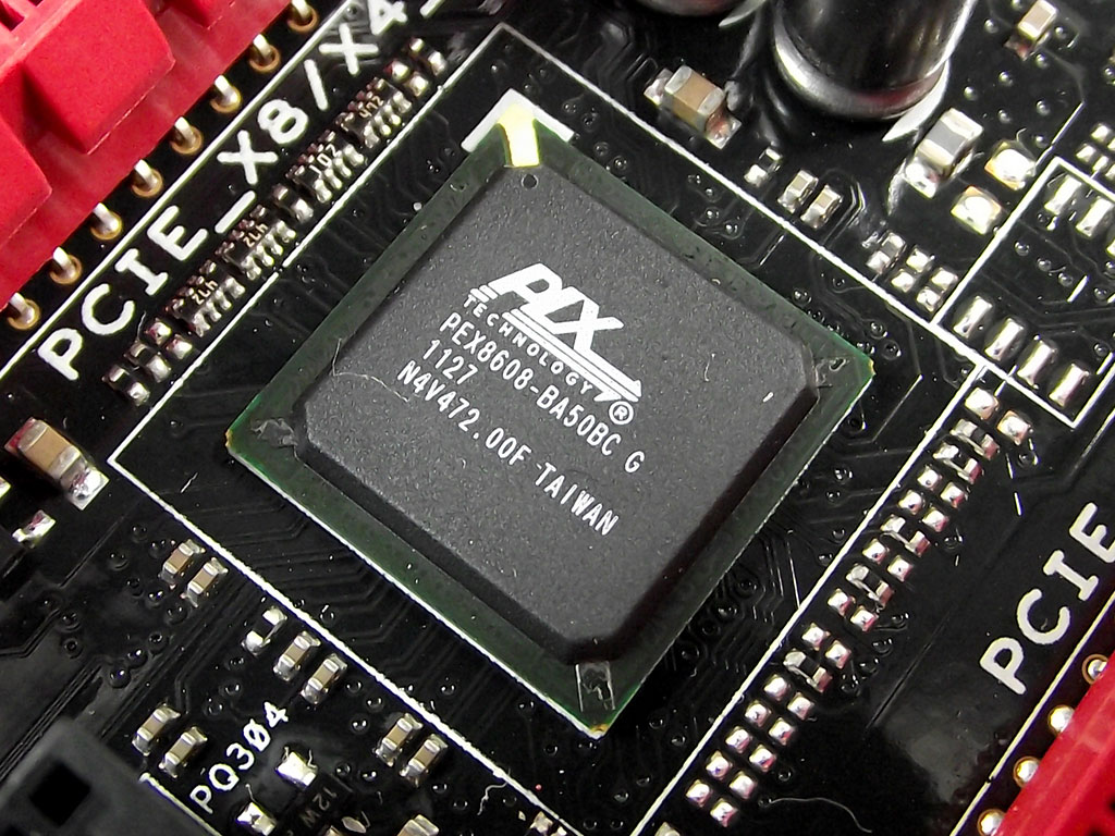
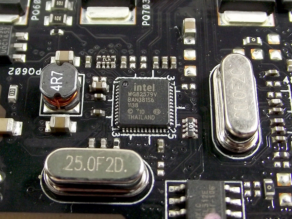
I found a PEX8608 PCIe 2.0 bridge chip by the PCIe x1 ports. I am not 100% sure what it's connected to, whether to those x1 slots or to external devices like the audio chip, but be that as it may, it does show that this board is filled to the brim with functionality, even more so than the Intel Z77 PCH itself can provide. LAN support, which does have a dedicated link to that Z77 PCH, is also provided by Intel, a WG82579V part that has proven to be faster and more efficient than some of the other options out there.
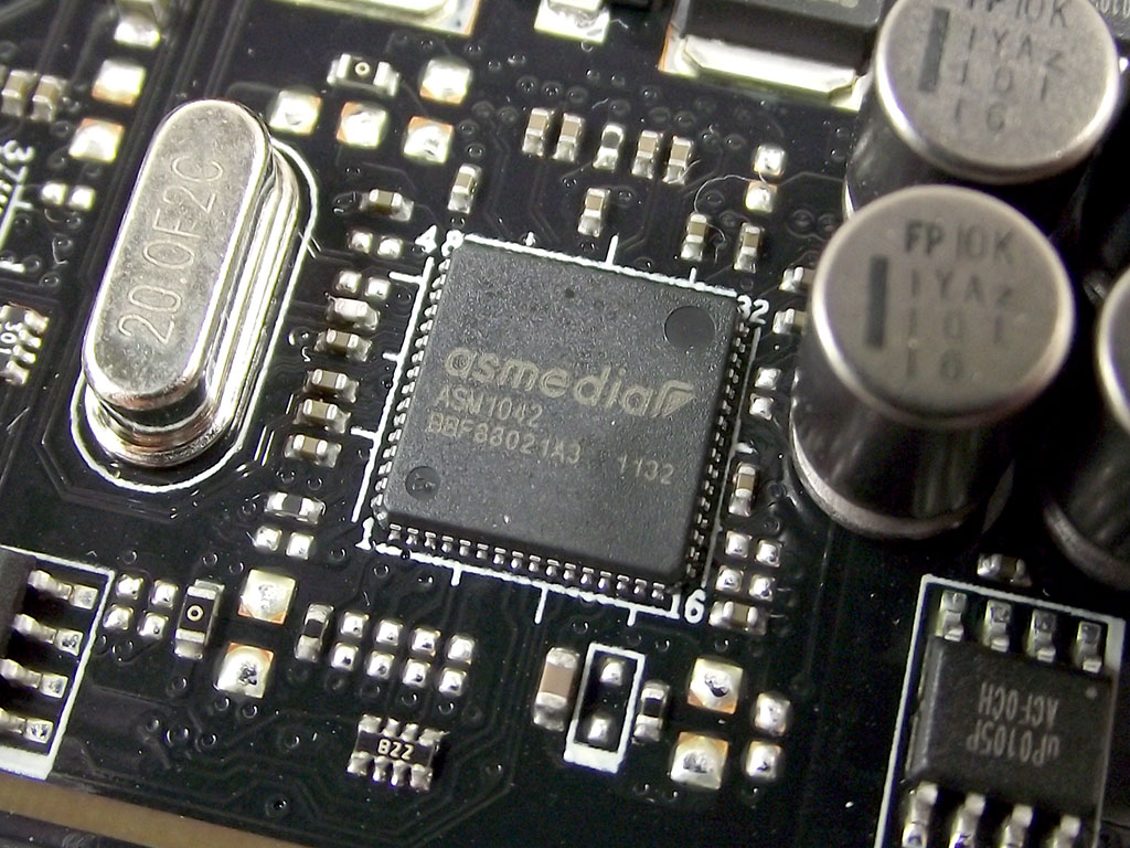


ASUS has been using ASMedia for external devices for some time now. It's no surprise to find several ASMedia-branded parts onboard the Maximus V Formula. I found USB 3.0, SATA 3 GB/s, and TMDS controllers by ASMedia.
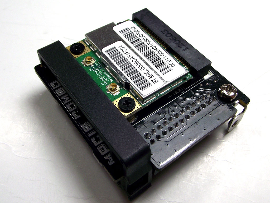
Of course, you've seen the eSATA port on the backplane, but I mentioned mSATA as well. A mSata connector, although I've shown pictures of the full board, cannot be found. It is, of course, contained on its own PCB, just as is the case with the Maximus V Gene, but, unlike the Maximus V Gene, the Maximus V Formula comes with a WiFi card pre-installed to the add-on card. This card itself has been updated a wee bit compared to the one found on the Maximus V Gene.

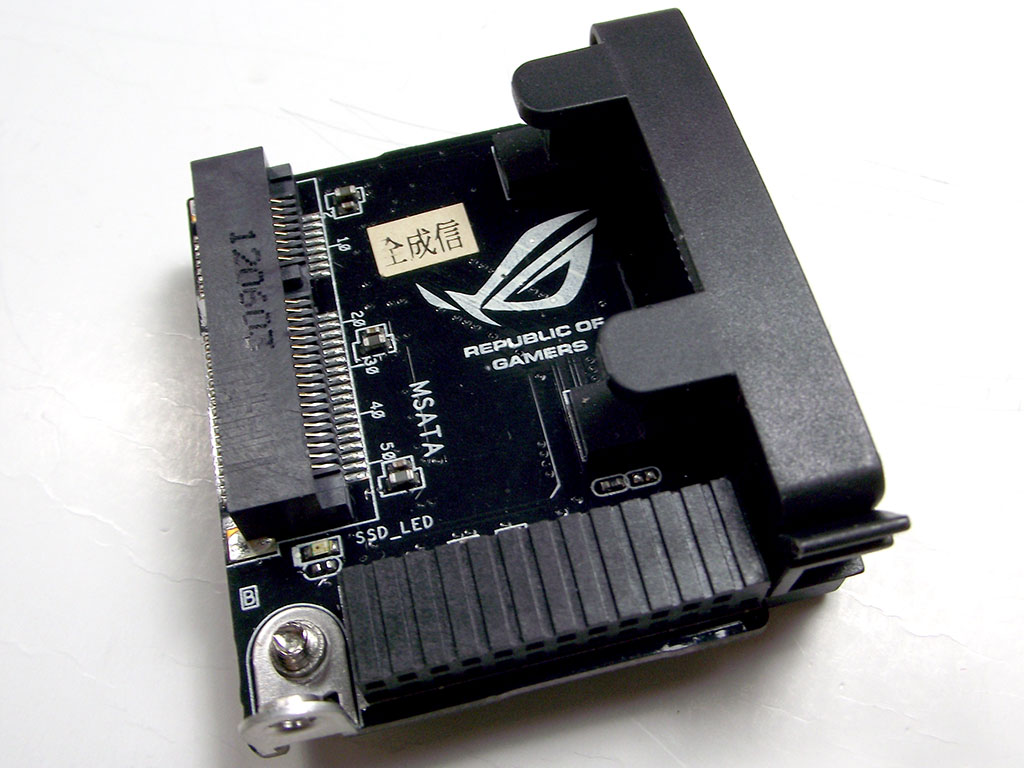
As you can see, my OCZ Nocti drive sits perfectly in the mSATA slot of the mPCIE Combo device. Both mSATA/WiFi capabilites are added to the board via the pin header shown above. The rear I/O plate has holes ready to be punched out so that you can install the antennas that connect to the mPCIE device with very short wires. I found these wires to be too short, and it was very difficult for me to install the complete unit into my case, something I hope ASUS fixes. The best advice I can mention here is to be sure you attach the antennas before mounting the board into the case, and to do the reverse when removing the board as well, which does become more complicated.

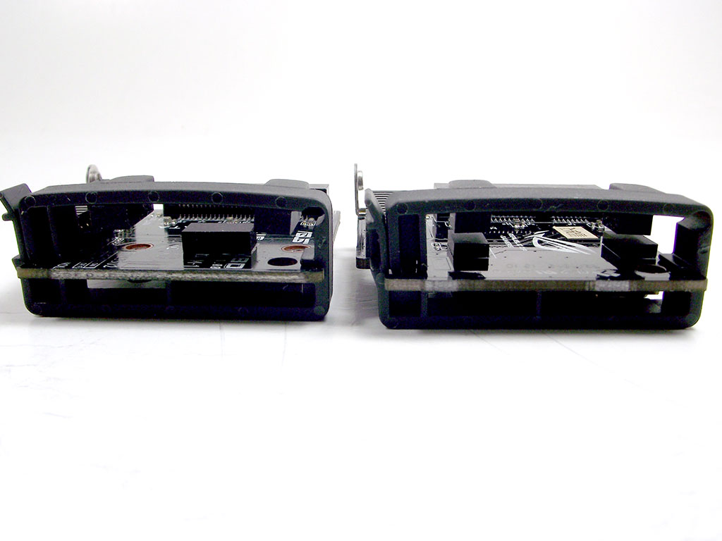
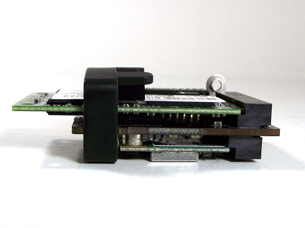
Above are both the module from the ASUS Maximus V Formula, and the one from the ASUS Maximus V Gene. In the first image, you can see both cards with the clips removed. One card has a single pad, while the other, newer one, has two pads. The older unit also has a Wake-On-Lan pin header that was removed. The second image shows both cards again, but with the mSATA retention clips in place, showing clearly how much more secure the clamping has become by just changing where the pads are situated. This was a very big issue I had with the Maximus V Gene and I was very happy to see that ASUS has revised the add-on card in such a way. I was also happy to see ASUS refer to these changes as an "mPCIE Combo Power Up!" on their product pages. ;)

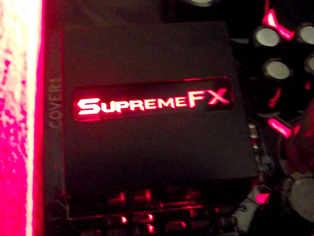
Moving over to audio, ASUS has really outdone themselves with an updated SupremeFX implementation that also includes a cover which shields the audio from electrical interference. They've also fitted the front-panel headphone connector with a fairly beefy amplifier, something I really did NOT expect.
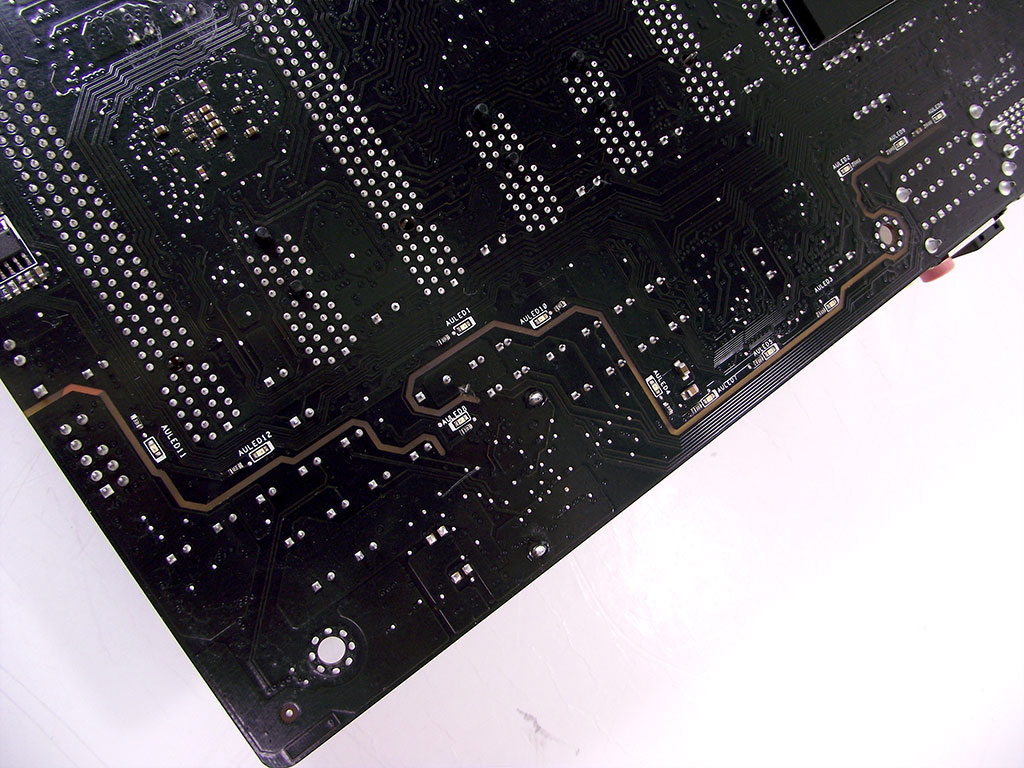

To further improve audio performance, ASUS has carried over an innovation I saw on the Maximus V Gene, pictured above. This includes a true PCB-level electrical isolation with very few points of contact between the audio portion and the rest of the PCB...only just as much as is required. To highlight this, and add some bling to the board, ASUS outfitted the rear of board with LEDs all along that line of electrical isolation with no copper on the PCB surface along the line, allowing the LEDS to shine through the PCB itself.
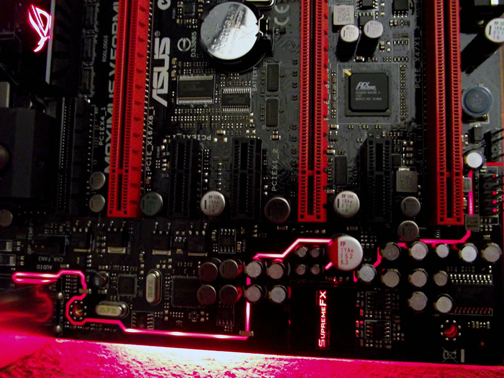
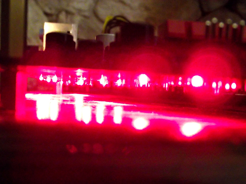
As you can see, the light that shines through the PCB is fairly muted, but does stand out quite nicely. The CODEC itself also has a couple of LED's under the cover, causing the logo on the metal cap to light up red as well. There are quite a few of these LEDs underneath the board. Looking at them directly, they are pretty bright, but the glow they give the Maximus V Formula is quite nice.


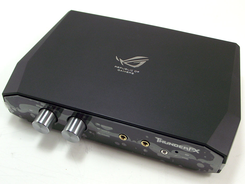
That's not all this board offers when it comes to audio since the black box, which was inside the inner box with the board itself, is nothing other than a USB headphone amp. It's not just for PC use either, being capable of working with the PS3 and XBOX360 by adding headphone support to those consoles easily. For PS3 use, simply connecting the USB cable is enough, but a few cables are needed for XBOX360 support since microphone support on that console is provided through the controller, while game audio is output from the rear of the console itself. It's very basic in outward appearance, but let me tell you, I could not have been more impressed by the audio it provides, never mind that I could have such great audio no matter how I game.
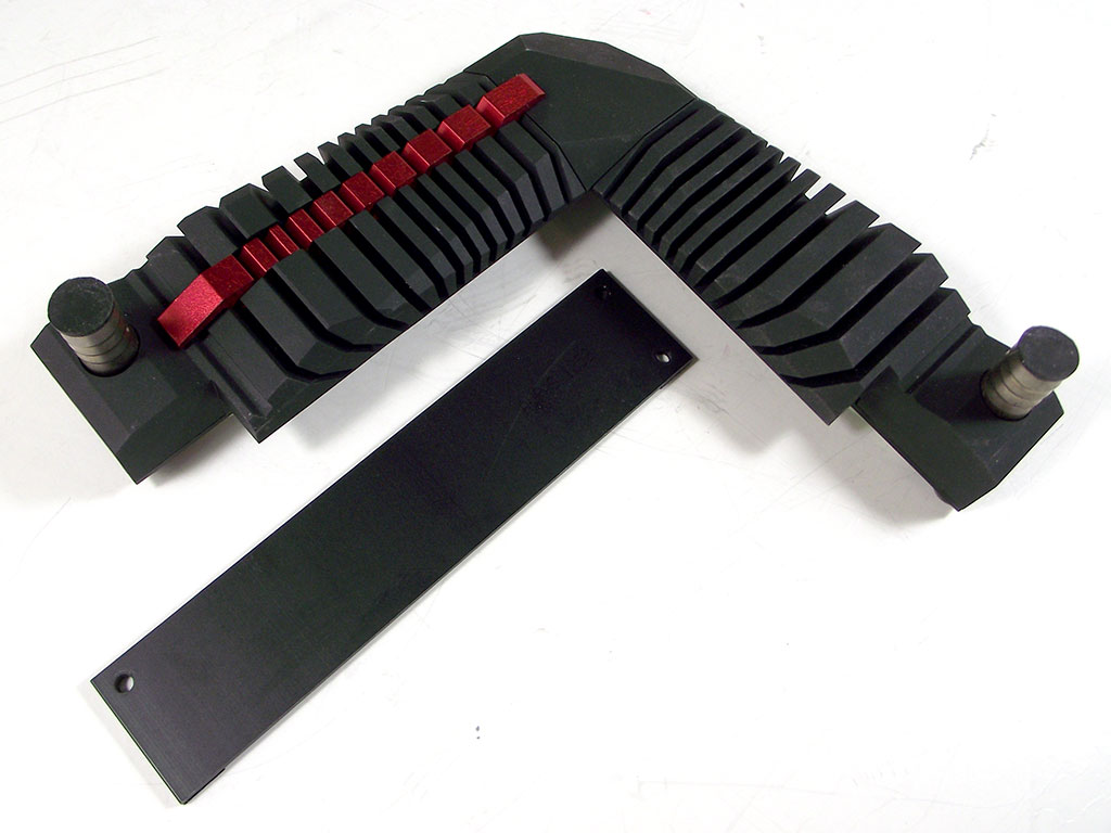
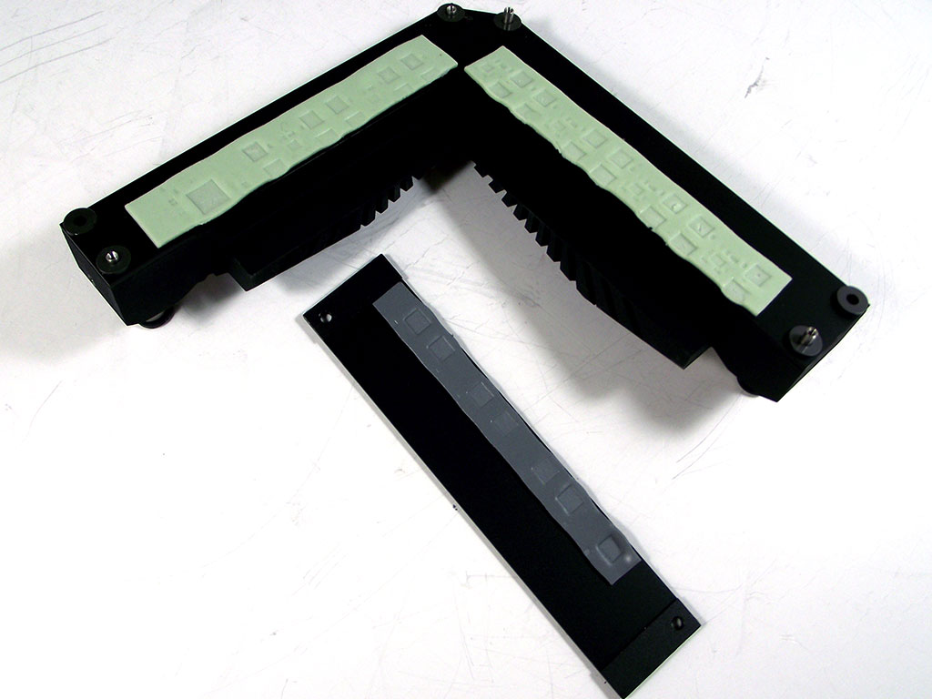
I did mention the coolers before, but a close-up presents a slightly different picture. The PCH cooler is all on its own, of course, just a big lump of aluminum with rounded edges. I actually couldn't get a good enough grip on it to remove it, and left it in place. VRM cooling is, of course, quite different, being a hybrid design that supports both air cooling and watercooling with an embedded channel that passes from end to end. With it removed from the board, we can see the excellent contact it makes with the board's VRM circuitry. Some might take issue with the size of fittings used, but I am perfectly happy with the 3/8" sizing. Even the backplate for the VRM cooler, which does contact several MOSFETs, is definitely overkill, with nearly three times the overall surface area compared to the space that the thermal pad uses.
May 10th, 2024 20:36 EDT
change timezone
Latest GPU Drivers
New Forum Posts
- Who here likes big monitors? 42inch and bigger gang? (1)
- Going from a 2070 to a 4070 ti super, should i uninstall drivers first? (19)
- 2024 and STILL no dark mode? (4)
- AM5 boot times improve RADICALLY with memory context restore enabled (35)
- NVME underperforming (3)
- Flash VBIOS to turn RX 580 2048SP into RX 570 (35)
- What are you playing? (20618)
- The Official Thermal Interface Material thread (1181)
- I don't think Ryzen 9900x3d is just being announced next month, I think it's launching next month. (26)
- Intel Core Ultra 9 185H - PROCHOT (3)
Popular Reviews
- Bykski CPU-XPR-C-I CPU Water Block Review - Amazing Value!
- CHERRY XTRFY M64 Pro Review
- ThundeRobot ML903 NearLink Review
- Corsair MP700 Pro SE 4 TB Review
- ZMF Caldera Closed Planar Magnetic Headphones Review
- Corsair iCUE Link RX120 RGB 120 mm Fan Review
- Upcoming Hardware Launches 2023 (Updated Feb 2024)
- AMD Ryzen 7 7800X3D Review - The Best Gaming CPU
- Finalmouse UltralightX Review
- ASUS Radeon RX 7900 GRE TUF OC Review
Controversial News Posts
- Intel Statement on Stability Issues: "Motherboard Makers to Blame" (264)
- AMD to Redesign Ray Tracing Hardware on RDNA 4 (206)
- Windows 11 Now Officially Adware as Microsoft Embeds Ads in the Start Menu (170)
- NVIDIA to Only Launch the Flagship GeForce RTX 5090 in 2024, Rest of the Series in 2025 (144)
- Sony PlayStation 5 Pro Specifications Confirmed, Console Arrives Before Holidays (119)
- AMD's RDNA 4 GPUs Could Stick with 18 Gbps GDDR6 Memory (114)
- NVIDIA Points Intel Raptor Lake CPU Users to Get Help from Intel Amid System Instability Issues (106)
- AMD Ryzen 9 7900X3D Now at a Mouth-watering $329 (104)