 0
0
G.SKILL F1-3200USU2-2GBHS PC3200 Review
Value and Conclusion »Test Setup
| Test System | |
|---|---|
| CPU: | AMD Athlon64 3200+ Winchester (multi lowered to 9) |
| Motherboard: | DFI LanParty NF4 UT Ultra-D (Bios 623-3) |
| Memory: | 2x 1024 MB G.SKILL F1-3200USU2-2GBHS PC3200 |
| Video Card: | ASUS Extreme N7800GT |
| Harddisk: | 2x Hitachi T7k250 160GB (Raid 0) |
| Power Supply: | Tagan 480W U22 |
| Software: | Windows XP SP2, ASUS VGA 81.89 |
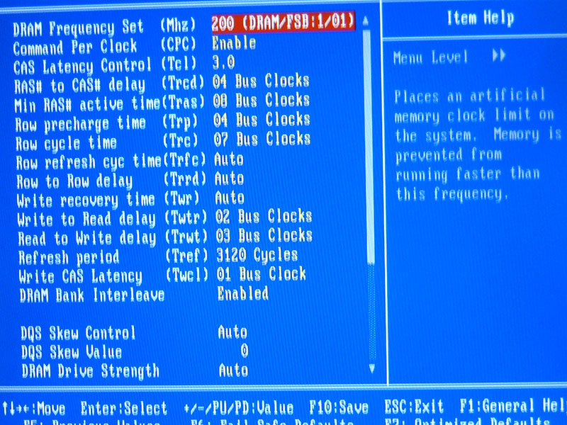
Alpha Timing settings in Bios:
We used same Timings as in the G.Skill F1-4000USU2-2GBHZ PC4000 review. Because both memories using the same chips.
Performance
At the beginning we tried to determine the best timings for 200 MHz. No matter what voltage we used the result was 2.5-3-3-8, like specified by G.Skill. CAS latency 2 was not possible. I also want to mention that the SPD timings were set incorrect to 3-3-3-8.The next step was overclocking the memory with stock timings. At 2.6V we could reach 246 MHz and with 2.8V 250 MHz. With more juice it was not possible to get more MHz.
So we lowered timings to 3-3-3-8. At 2.6V the result was the same as with 2.5-3-3-8, 246 MHz. But with 2.8V we could get 6 MHz more (256 MHz)
Now we changed to 3-4-4-8 and got 262 MHz with 2.6V and 272 MHz with 2.8V. That's a 36% overclock. Only 3 MHz less than the big brother G.Skill 4000HZ which is more expensive.
We also tried higher voltage on all timings, but the memory did not benefit from it.
In comparison to the G.SKILL 4000HZ with same chips and same PCB, the 3200HS loves a little bit higher voltage (2.8V), the 4000HZ does not. Maybe the 3200HS have a newer batch of chips.
But do not forget that 2GB always overclocks less than 1GB because of higher density.
The last test "JEDEC DDR-400A" is for comparison with a generic DDR module running at JEDEC standard timings.
| G.SKILL F1-3200USU2-2GBHS PC3200 | ||||||||
|---|---|---|---|---|---|---|---|---|
| CPU Clock & Memory Ratio | Memory Speed | Memory Timings | Everest Read | Everest Write | Everest Latency | Quake 3 Timedemo | 3DMark 2001SE | SuperPi Mod 1M |
| 9 x 200 1:1 | 200 MHz | 2.5-3-3-8 2.6V | 5699 MB/s | 2189 MB/s | 52.2 ns | 395.0 fps | 20931 | 44.62 s |
| 9 x 246 1:1 | 246 MHz | 2.5-3-3-8 2.6V | 6934 MB/s | 2629 MB/s | 42.1 ns | 483.5 fps | 24596 | 37.38 s |
| 9 x 250 1:1 | 250 MHz | 2.5-3-3-8 2.8V | 7155 MB/s | 2665 MB/s | 40.7 ns | 492.2 fps | 24914 | 37.72 s |
| 9 x 246 1:1 | 246 MHz | 3-3-3-8 2.6V | - | - | - | - | - | - |
| 9 x 256 1:1 | 256 MHz | 3-3-3-8 2.8V | 7200 MB/s | 2674 MB/s | 42.7.0 ns | 495.1 fps | 25250 | 36.52 s |
| 9 x 262 1:1 | 262 MHz | 3-4-4-8 2.6V | 7180 MB/s | 2710 MB/s | 44.0 ns | 497.3 fps | 22590 | 36.14 s |
| 9 x 272 1:1 | 272 MHz | 3-4-4-8 2.8V | 7530 MB/s | 2740 MB/s | 42.1 ns | 515.9 fps | 25675 | 34.80 s |
| JEDEC DDR-400A | 200 MHz | 2.5-3-3-8 2.6V | 5699 MB/s | 2189 MB/s | 52.2 ns | 395.0 fps | 20931 | 44.62 s |

SuperPi - 272 MHz; 3-4-4-8; 2.8V
Benchmarks


For easier comparison with other modules, we set the maximum voltage required for the best result (here 2.8V; max 3.1V) and tested until we found the highest clock frequency and fastest timings for this memory. The benchmarks Everest Read, Everest Write and Quake 3 were run. We then calculated the performance increase in percent compared to some standard DDR-400 memory running at JEDEC standard timings (2.5-3-3-8). The average percentage of the three benchmarks is listed in following table:

Apr 26th, 2024 06:30 EDT
change timezone
Latest GPU Drivers
New Forum Posts
- What's your latest tech purchase? (20347)
- Share your AIDA 64 cache and memory benchmark here (2918)
- Secure boot already open help (1)
- What are you playing? (20535)
- Best SSD for system drive (83)
- TPU's Nostalgic Hardware Club (18472)
- Last game you purchased? (258)
- Alphacool CORE 1 CPU block - bulging with danger of splitting? (22)
- Nvidia CMP 100-210 or 100HX (GV100 GPU) (9)
- Horizontal black lines popping up on my screen? (7)
Popular Reviews
- HYTE THICC Q60 240 mm AIO Review
- Alienware Pro Wireless Gaming Keyboard Review
- MOONDROP x Crinacle DUSK In-Ear Monitors Review - The Last 5%
- Upcoming Hardware Launches 2023 (Updated Feb 2024)
- Thermalright Phantom Spirit 120 EVO Review
- RTX 4090 & 53 Games: Ryzen 7 5800X vs Ryzen 7 5800X3D Review
- ASUS Radeon RX 7900 GRE TUF OC Review
- RTX 4090 & 53 Games: Core i9-13900K vs Ryzen 7 5800X3D Review
- NVIDIA RTX 4090: 450 W vs 600 W 12VHPWR - Is there any notable performance difference?
- FiiO K19 Desktop DAC/Headphone Amplifier Review
Controversial News Posts
- Windows 11 Now Officially Adware as Microsoft Embeds Ads in the Start Menu (123)
- Sony PlayStation 5 Pro Specifications Confirmed, Console Arrives Before Holidays (117)
- NVIDIA Points Intel Raptor Lake CPU Users to Get Help from Intel Amid System Instability Issues (106)
- AMD "Strix Halo" Zen 5 Mobile Processor Pictured: Chiplet-based, Uses 256-bit LPDDR5X (101)
- US Government Wants Nuclear Plants to Offload AI Data Center Expansion (98)
- AMD's RDNA 4 GPUs Could Stick with 18 Gbps GDDR6 Memory (89)
- Developers of Outpost Infinity Siege Recommend Underclocking i9-13900K and i9-14900K for Stability on Machines with RTX 4090 (85)
- Windows 10 Security Updates to Cost $61 After 2025, $427 by 2028 (84)