 16
16
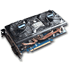
Galaxy GeForce GTS 250 1 GB Review
Test Setup »A Closer Look
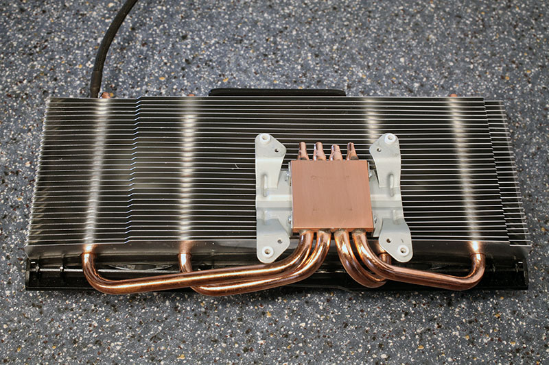

The cooler uses a copper base that is connected to a large heatsink via four heatpipes.

This small metal heatsink is sitting on top of the voltage regulators helping to keep them cool. Since it is located almost directly below a fan there is plenty of airflow around the heatsink.
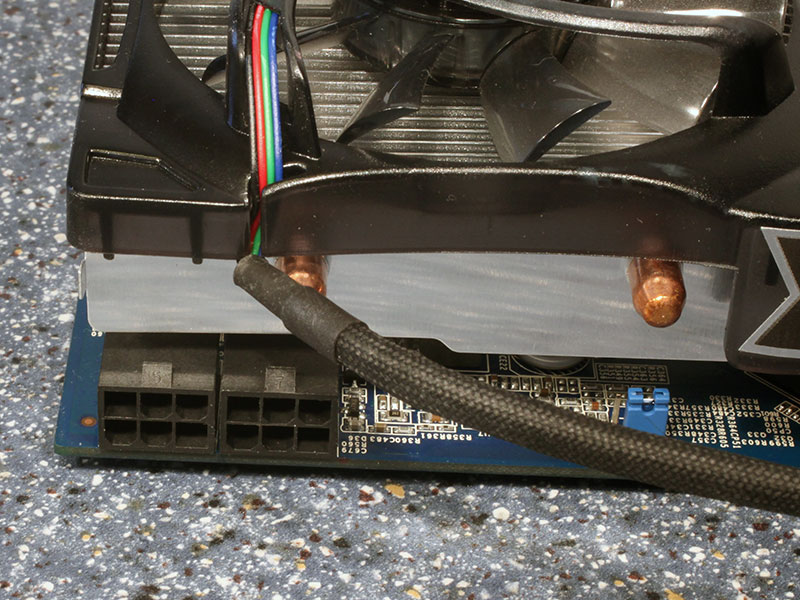
The card has two six-pin power connectors, both are required for operation of the card.

The GDDR3 memory chips are made by Hynix and carry the model number H5RS1H23MFR-N2C. With a latency of 0.8 ns, they are specified to run at 1200 MHz.

Galaxy uses a voltage regulator from Richtek on their card. Unfortunately this design does not allow software based voltage control (like on the much more expensive Volterra regulators).


When I first removed the cooler I was greeted by this thermal paste mess. Looks like the cooler had been removed a couple of times before. After some cleanup we get to see the G92 in all its beauty. It is made in a 55 nm process with 754 million transistors.
Apr 26th, 2024 22:08 EDT
change timezone
Latest GPU Drivers
New Forum Posts
- FINAL FANTASY XIV: Dawntrail Official Benchmark (73)
- Your PC ATM (34509)
- Rare GPUs / Unreleased GPUs (1877)
- looking to build a new system and im considering asrock brand but i have some doubts/concerns. (15)
- AAF Optimus DCH Audio Modded Driver for Windows 10/11 - For ALL HDAUDIO Enumerator Chips (652)
- Help me identify rx 580 card ? (0)
- Strange system crashes out of nowhere help (9)
- What phone you use as your daily driver? And, a discussion of them. (1494)
- Secure boot already open help (11)
- TechPowerUp Screenshot Thread (MASSIVE 56K WARNING) (4213)
Popular Reviews
- Ugreen NASync DXP4800 Plus Review
- HYTE THICC Q60 240 mm AIO Review
- Quick Look: MOONDROP CHU 2 Budget In-Ear Monitors
- MOONDROP x Crinacle DUSK In-Ear Monitors Review - The Last 5%
- Thermalright Phantom Spirit 120 EVO Review
- Upcoming Hardware Launches 2023 (Updated Feb 2024)
- CeBIT 2008: Akasa Review
- CeBIT 2008: Cyber E Sport Review
- Alienware Pro Wireless Gaming Keyboard Review
- Gigabyte GeForce RTX 4070 Ti Super Gaming OC Review
Controversial News Posts
- Windows 11 Now Officially Adware as Microsoft Embeds Ads in the Start Menu (135)
- Sony PlayStation 5 Pro Specifications Confirmed, Console Arrives Before Holidays (117)
- NVIDIA Points Intel Raptor Lake CPU Users to Get Help from Intel Amid System Instability Issues (106)
- AMD "Strix Halo" Zen 5 Mobile Processor Pictured: Chiplet-based, Uses 256-bit LPDDR5X (103)
- US Government Wants Nuclear Plants to Offload AI Data Center Expansion (98)
- AMD's RDNA 4 GPUs Could Stick with 18 Gbps GDDR6 Memory (95)
- Developers of Outpost Infinity Siege Recommend Underclocking i9-13900K and i9-14900K for Stability on Machines with RTX 4090 (85)
- Windows 10 Security Updates to Cost $61 After 2025, $427 by 2028 (84)