 55
55
Ivy Bridge PCI-Express Scaling with HD 7970 and GTX 680 Review
Test Setup »Introduction

The last time we did an article on PCI-Express scaling, was when graphics cards were finally able to saturate the bandwidth of PCI-Express x16. Not only was it a time when PCI-Express 2.0 was prevalent, but also when the first DirectX 11 GPU hit the market, and that was over six years into the introduction of the PCI-Express bus interface. Since 2009, thanks to fierce competition between NVIDIA and AMD, GPU performance levels have risen at a faster rate than ever, and the latest generation of high-end GPUs launched by the two GPU rivals adds support for the new PCI-Express 3.0 interface. The new interface sprung new questions from users like "Do I need a new motherboard to run a PCI-Express 3.0 card?", "Will my new PCI-Express 3.0 card be much slower on an older motherboard?" or "My motherboard supports only x8 for multiple cards, will performance suck?"
The industry's first PCI-Express 8 GT/s-capable platform was released last year, with Intel's Sandy Bridge-E. SB-E isn't officially PCI-Express 3.0-certified; while AMD Southern Islands GPUs can function in PCI-Express 3.0 on the platform, NVIDIA's GeForce Kepler family of GPUs, so far, can't. The 22 nm Core processor family, codenamed Ivy Bridge, however, settles the issue by providing a PCI-Express 3.0-certified root-complex, and GPUs from both sides of the fence are tested to work on the new mode. PCI-Express 3.0 close to doubles the data bandwidth available to a connected device, per lane.
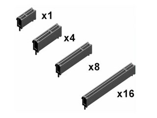
While PCI-Express 1.0 pushes 250 MB/s per direction, PCI-Express 2.0 pushes 500 MB/s, and PCI-Express 3.0 doubles that to 1 GB/s. While the resulting absolute bandwidth of PCI-Express 3.0 x16, 32 GB/s, might seem overkill, the ability to push that much data per lane could come to the rescue of configurations such as 8-lanes (x8) and 4-lanes (x4). Another impressive feature of Ivy Bridge Core processors, provided they're paired with Intel Z77 Express chipset, is that the second x8 link from the CPU root complex can be split as two x4 links, making x8/x4/x4 possible, giving some motherboards 3-way SLI and CrossFireX capabilities without clogging the DMI chipset bus (that 4 GB/s pipe between the CPU and chipset), which is better left untouched by graphics cards to help with today's bandwidth-hungry SSDs.

In this review, we test the impact of running the AMD Radeon HD 7970 and the GeForce GTX 680 on Intel Ivy Bridge PCI-Express slots that are electrically PCI-Express x16, x8 and x4. We tested all three generations of the PCI-Express interface: 1.1, 2.0 and 3.0.
This review is made possible thanks to an awesome BIOS option given to us by ASUS ROG Maximus V Gene motherboard, which allows us to toggle the CPU's PCI-Express root complex between PCI-Express 1.0, 2.0, and 3.0 modes. To modify the number of lanes available to the GPU, we used common plastic adhesive tape.
For your reference, we wrote similar articles in the past: GTX 480 PCIe Scaling, HD 5870 PCIe Scaling.
Apr 27th, 2024 04:33 EDT
change timezone
Latest GPU Drivers
New Forum Posts
- wireless mic for pc (0)
- Ryzen Owners Zen Garden (7245)
- My mouse randomly stops working (2)
- Horizontal black lines popping up on my screen? (14)
- Should I install Windows 10 or 11 for my new device (4)
- MSI Stealth GS65 9SF settings after repaste (0)
- Which terminal emulator do you use the most? (10)
- Browser startup performance test (4)
- The TPU UK Clubhouse (24789)
- List of NPU-optimized apps and games (0)
Popular Reviews
- Ugreen NASync DXP4800 Plus Review
- HYTE THICC Q60 240 mm AIO Review
- MOONDROP x Crinacle DUSK In-Ear Monitors Review - The Last 5%
- Upcoming Hardware Launches 2023 (Updated Feb 2024)
- Thermalright Phantom Spirit 120 EVO Review
- FiiO K19 Desktop DAC/Headphone Amplifier Review
- Quick Look: MOONDROP CHU 2 Budget In-Ear Monitors
- AMD Ryzen 7 7800X3D Review - The Best Gaming CPU
- Alienware Pro Wireless Gaming Keyboard Review
- Corsair iCUE Link XC7 RGB Elite CPU Water Block Review
Controversial News Posts
- Windows 11 Now Officially Adware as Microsoft Embeds Ads in the Start Menu (137)
- Sony PlayStation 5 Pro Specifications Confirmed, Console Arrives Before Holidays (117)
- NVIDIA Points Intel Raptor Lake CPU Users to Get Help from Intel Amid System Instability Issues (106)
- AMD "Strix Halo" Zen 5 Mobile Processor Pictured: Chiplet-based, Uses 256-bit LPDDR5X (103)
- US Government Wants Nuclear Plants to Offload AI Data Center Expansion (98)
- AMD's RDNA 4 GPUs Could Stick with 18 Gbps GDDR6 Memory (95)
- Developers of Outpost Infinity Siege Recommend Underclocking i9-13900K and i9-14900K for Stability on Machines with RTX 4090 (85)
- Windows 10 Security Updates to Cost $61 After 2025, $427 by 2028 (84)