 125
125
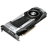
NVIDIA GeForce GTX 1070 8 GB Review
Test Setup »A Closer Look

NVIDIA's new thermal solution cools all components: GPU, memory chips, and voltage regulation circuitry. While the GTX 1080 uses a vapo-chamber baseplate for the GPU, the GTX 1070 uses three copper heatpipes instead.


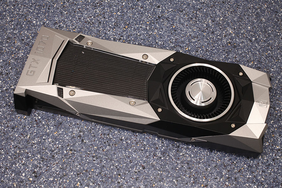
As mentioned before, NVIDIA has updated their backplate design to be thinner than ever, providing more airflow to the second card in an SLI configuration. Should you want to improve airflow even more, the backplate is now made up of two separately removable pieces, and you will not have to remove the main cooler. The pictures above show the removal of each of these pieces. The backplate on top of the GPU has three thermal pads that cover some thicker components for short-circuit protection.

With the GeForce GTX 1070 and GTX 1080, NVIDIA is using a single 8-pin power connector for the first time. While providing the same power as two 6-pin connectors, it simplifies installation and cable routing. This input configuration is specified for up to 225 watts of power draw.

In order to disassemble the card, you have to remove these tiny screws; no, they are not nuts since the hole inside is threaded so the screws used to attach the backplate can go in. Without the right tool, these are incredibly difficult to remove. In my GTX 1080 review, I used pliers, bot now have the correct tool, which made things much easier.
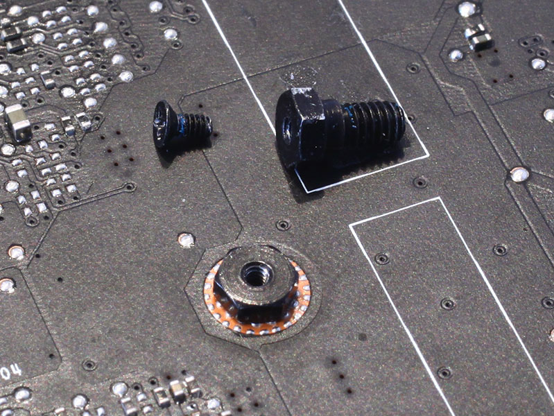
NVIDIA Pascal is introducing a new voltage controller by uPI, the uP 9511P. Its exact feature set is currently unknown.

The GDDR5 memory chips are made by Samsung and carry the model number K4G80325FB-HC25. They are specified to run at 2000 MHz (8000 MHz GDDR5 effective). This is the biggest change compared to the GTX 1080, which uses GDDR5X memory.

NVIDIA's GP104 graphics processor is the first consumer chip using the Pascal architecture. It is produced on a 16 nm process at TSMC, Taiwan, with a transistor count of 7.1 billion and a die size of 314 mm².
May 2nd, 2024 22:13 EDT
change timezone
Latest GPU Drivers
New Forum Posts
- Need help with a persistent infection possible rootkit or other device. (11)
- ARDIYES RX 580 8gb Graphics Card (19)
- need help with power limiting my i7-8750h (9)
- The Official Thermal Interface Material thread (1136)
- 7800x3d $216 in bundle at Microcenter (31)
- FINAL FANTASY XIV: Dawntrail Official Benchmark (77)
- What's your latest tech purchase? (20415)
- Have you got pie today? (16324)
- WCG Daily Numbers (12504)
- Milestones (13878)
Popular Reviews
- HYTE THICC Q60 240 mm AIO Review
- ASRock NUC BOX-155H (Intel Core Ultra 7 155H) Review
- Montech Sky Two GX Review
- Ugreen NASync DXP4800 Plus Review
- Upcoming Hardware Launches 2023 (Updated Feb 2024)
- Team Group T-Force Vulcan ECO DDR5-6000 32 GB CL38 Review
- Meze Audio LIRIC 2nd Generation Closed-Back Headphones Review
- MOONDROP x Crinacle DUSK In-Ear Monitors Review - The Last 5%
- AMD Ryzen 7 7800X3D Review - The Best Gaming CPU
- Logitech G Pro X Superlight 2 Review - Updated with 4000 Hz Tested
Controversial News Posts
- Intel Statement on Stability Issues: "Motherboard Makers to Blame" (229)
- Windows 11 Now Officially Adware as Microsoft Embeds Ads in the Start Menu (166)
- Sony PlayStation 5 Pro Specifications Confirmed, Console Arrives Before Holidays (117)
- AMD's RDNA 4 GPUs Could Stick with 18 Gbps GDDR6 Memory (114)
- NVIDIA Points Intel Raptor Lake CPU Users to Get Help from Intel Amid System Instability Issues (106)
- AMD "Strix Halo" Zen 5 Mobile Processor Pictured: Chiplet-based, Uses 256-bit LPDDR5X (103)
- AMD Ryzen 9 7900X3D Now at a Mouth-watering $329 (103)
- TechPowerUp Hiring: Reviewers Wanted for Motherboards, Laptops, Gaming Handhelds and Prebuilt Desktops (93)