 344
344
NVIDIA GeForce GTX 680 Kepler 2 GB Review
Value & Conclusion »Manual overclocking
On the previous page we discussed how NVIDIA's GPU Bost works. If you just skipped here, go back one page and read it. It's really important to understand the basics of the dynamic clock adjustments before trying to understand the implications for manual overclocking.Manually setting a specific GPU clock on the GeForce GTX 680 is not possible. You can only define a certain offset that the dynamic overclocking algorithm will _try_ to respect. If the card runs into the power limit or something else comes up, the clocks will be lower than requested. Think of it more as a "best effort plzplz" value than a hard setting.
NVIDIA has defined a hard limit of +549 MHz for the clock offset, which will certainly upset some extreme overclockers with liquid nitrogen. As mentioned several times before, there is no way to turn off dynamic clocking, which means there is no way to go back to the classic overclocking method. Also directly accessing hardware to write clocks to the clock generator won't work as the algorithm in the driver will instantly overwrite it with what it thinks is right. The clock offset simply acts as additional input variable for the dynamic clock algorithm which also takes into account things like power consumption, temperature and GPU load.
This means that no matter how hard you try using clock offsets, power limits and voltage settings, the card will always reduce clocks when it thinks it has to.
Increased GPU Clock
I tried running at various clock offsets to check what real-life performance boost they offer, because the clock offset is only a target value and actual clocks during gaming may differ, despite the selected clock offset.I picked +50 MHz and +100 MHz as both are rock stable and they provide some insight into how well clock scaling will work. Please note, both these runs were with board power limit set to default.

Using a small overclock of just 50 MHz we see immediately that performance gains are relatively small with only 1.3% faster than the GTX 680 running its default boost clock algorithm.

Given a selected clock offset of +50 MHz, we would expect clocks between 1056 MHz (base clock + 50 MHz) and 1150 MHz (highest dynamic clock + 50 MHz). While the majority of clocks are bunched up in that region indeed, we do see a good amount of clocks below 1056 MHz, all the way down to the default base clock of 1006 MHz and even below.
These unexpected clocks can be explained by dynamic overclocking reducing clock speeds because a certain game scene causes it to run into the TDP power limit, or similar situations. Increased temperature from overclocking alone can not account for the difference, as it can only reduce clocks by 40 MHz, which would still give us a lowest clock of 1016 MHz.
Next I tried increasing clocks further using an offset of +100 MHz.

Here we see 2.9% real life performance gained. Also note the increased amount of upward spikes in Shogun 2, BF3 and Dragon Age 2, which are caused by games that love to run higher clocks, yet are not blocked by the power limiter from doing so.

The clock distribution shows an even more stretched out range of clocks. Again, ranging from below 1000 MHz, through 1106 MHz (which would be our new base clock with the offset taken into account), all the way up to a maximum of 1215 MHz.
Increased Memory Clock
I ran a quick test, bumping memory clock by +100 MHz to 1603 MHz using the clock offset option.
As the data shows, memory clock is constant during 3D, the drops you see are from when the card switches to 2D clocks between tests.
This means that dynamic overclocking is only active for the GPU clock, which will make things a bit easier.
Voltage Tuning
Adjusting voltage has become a little bit more difficult due to dynamic overclocking. It seems that the NVIDIA driver enforces a voltage minimum, which ensures dynamic OC is stable. Voltage selection to higher levels is possible, but limited to the driver maximum of 1.175 V. The voltage controller on the board has no support for I2C, so it can not be programmed directly.For example, if the dynamic clock algorithm decides it wants to run the card at 1.125 V, then the voltage will be 1.125 V, despite any manually set voltage between 0.825 V (the available minimum) and 1.125 V.
Once you manually set 1.137 V (one step up from 1.125 V), this voltage will become active. However, should the dynamic OC algorithm decide that it needs more juice because it wants to set a higher clock, your setting will be overriden for the time that this clock/voltage combination is active.
As mentioned before, each card's individual set of voltages depends on a value stored in the GPU during production time, so actual voltages may differ. The mechanism of voltage control will be the same however.
Putting it all together
So now that we know how overclocking works, let's put it to some good use.Finding maximum clocks is similar as before, except that you have to search for a new stress testing application as Furmark will run at significantly reduced clocks due to power limit, so the actual requested clocks will not be tested. Further, 3DMark11 does not seem a good choice either, as it let me run much higher clocks than were stable in other tests. Out of the games in our benchmark suite I found Unigine Heaven to be the best for stability testing. It also notifies you when the card crashes, causing a driver reset. If that happens, it's best that you restart the system to make sure it is fully stable and working well, before trying a slightly reduced clock frequency.
Personally I think with the latest generation of cards from both AMD and NVIDIA, that both have some sort of power limiting system that messes with your overclock, the best stress testing is playing your favorite games. So go ahead and find what looks like a stable set of clocks, set them and don't worry about them until you see rendering errors or crashes during your gaming, then take the clocks down a notch and repeat. This is also more efficient and more fun than staring at stability tests all day.
And don't forget to set the board power limit to +32%, to ensure the power limit will not drop down your clocks. We did so for all further OC testing.
Maximum OC

Maximum stable clocks of our card are 1159 MHz GPU / +153 MHz clock offset (15% overclock) and 1833 MHz Memory (22% overclock). (HD 7970 review: +16% / +25%)
Both overclocks are great, especially seeing memory overclock so far is nice. Previous Fermi generation GPUs did much worse here. It's also good to see that there is still some headroom left in the cards for manual tweaking and dynamic OC didn't eat up the whole OC potential.
Please note that the dynamic overclocking mechanism will automatically adjust GPU clocks to lower level in case it thinks it is required to do so. Also it will increase GPU voltage to a level that's guaranteed to work with the selected clock - when possible. Once it hits the maximum voltage, it will not increase voltage any further. This implies that basic overclocking is more stable now, but once you go beyond the qualified clock range, stability testing is still required.
Overclocked Performance
Using these clock frequencies we ran the 1920x1200 resolution tests of our benchmarking suite to evaluate real life performance gains. I also added a manually overclocked (but not overvolted) HD 7970 reference design, so you can see what to expect when manual overclocking is taken into account for both cards. Both results are directly comparable, higher vertical position implies higher performance in that specific game. The 0% line is the performance that we saw from the non-overclocked GTX 680, just running the default dynamic OC algorithm, without any clock offsets or power limit change.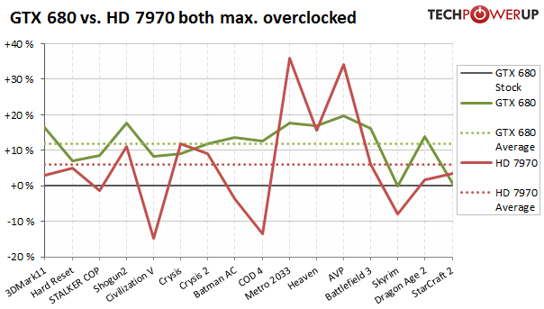
So even when both cards are manually tweaked to deliver maximum performance, NVIDIA's GeForce GTX 680 is still on top. Overclocking the Radeon HD 7970 does give it a nice performance boost though, which allows it to surpass the out-of-the-box GTX 680 experience.
To be honest, when I started overclocking GTX 680 I was extremely sceptical how well manual overclocking would work, and how much dynamic OC would interfere. As the previous pages have shown, the overclocking process is more complex, there are a few gotchas to consider, but it is still possible to get a significant amount of extra performance out of the card - in our case +11.9% vs. the stock GTX 680.
Temperatures

Temperatures are decent. It would have been nice to see lower load temperatures on the GTX 680, but this doesn't seem viable given the noise levels of the card. As mentioned on the previous page, lower temperatures directly translate into higher performance, as dynamic overclocking reduces clocks when temperatures get high.
Clock Profiles
Modern graphics cards have several clock profiles that are selected to balance power draw and performance requirements.The following table lists the clock settings for important performance scenarios and the GPU voltage that we measured. We measure on the pins of a coil or capacitor near the GPU voltage regulator.
| Core Clock | Memory Clock | GPU Voltage (measured) | |
|---|---|---|---|
| Desktop | 324 MHz | 162 MHz | 0.99 V |
| Multi-Monitor | 550 MHz | 1502 MHz | 0.99 V |
| Blu-ray Playback | 549 MHz | 405 MHz | 0.99 V |
| 3D Load | 1006 - 1111 MHz | 1502 MHz | 1.20 V |
Apr 27th, 2024 03:18 EDT
change timezone
Latest GPU Drivers
New Forum Posts
- Should I install Windows 10 or 11 for my new device (1)
- The TPU UK Clubhouse (24789)
- List of NPU-optimized apps and games (0)
- rx 6500 xt anisotropic filtering not working (1)
- What phone you use as your daily driver? And, a discussion of them. (1497)
- Alphacool CORE 1 CPU block - bulging with danger of splitting? (35)
- What are you playing? (20541)
- Safe memory overclock for the rtx 4050? (8)
- Help me identify rx 580 card ? (1)
- Your PC ATM (34511)
Popular Reviews
- Ugreen NASync DXP4800 Plus Review
- HYTE THICC Q60 240 mm AIO Review
- MOONDROP x Crinacle DUSK In-Ear Monitors Review - The Last 5%
- Upcoming Hardware Launches 2023 (Updated Feb 2024)
- Thermalright Phantom Spirit 120 EVO Review
- Quick Look: MOONDROP CHU 2 Budget In-Ear Monitors
- FiiO K19 Desktop DAC/Headphone Amplifier Review
- AMD Ryzen 7 7800X3D Review - The Best Gaming CPU
- Alienware Pro Wireless Gaming Keyboard Review
- Corsair iCUE Link XC7 RGB Elite CPU Water Block Review
Controversial News Posts
- Windows 11 Now Officially Adware as Microsoft Embeds Ads in the Start Menu (136)
- Sony PlayStation 5 Pro Specifications Confirmed, Console Arrives Before Holidays (117)
- NVIDIA Points Intel Raptor Lake CPU Users to Get Help from Intel Amid System Instability Issues (106)
- AMD "Strix Halo" Zen 5 Mobile Processor Pictured: Chiplet-based, Uses 256-bit LPDDR5X (103)
- US Government Wants Nuclear Plants to Offload AI Data Center Expansion (98)
- AMD's RDNA 4 GPUs Could Stick with 18 Gbps GDDR6 Memory (95)
- Developers of Outpost Infinity Siege Recommend Underclocking i9-13900K and i9-14900K for Stability on Machines with RTX 4090 (85)
- Windows 10 Security Updates to Cost $61 After 2025, $427 by 2028 (84)