erocker
*
- Joined
- Jul 19, 2006
- Messages
- 43,636 (6.28/day)
| Processor | AMD Ryzen 7 7800X3D |
|---|---|
| Motherboard | ASUS TUF x670e-Plus Wifi |
| Cooling | EK AIO 360. Phantek T30 fans. |
| Memory | 64GB G.Skill 6000Mhz |
| Video Card(s) | Asus RTX 4090 |
| Storage | WD/Samsung m.2's |
| Display(s) | LG C2 Evo OLED 42" |
| Case | Fractal Design North |
| Audio Device(s) | Topping E70 DAC, SMSL SP200 Amp, Adam Audio T5V's, Hifiman Sundara's. |
| Power Supply | FSP Hydro Ti PRO 1000W |
| Mouse | Razer Basilisk V3 Pro |
| Keyboard | Epomaker 84 key |
| Software | Windows 11 Pro |
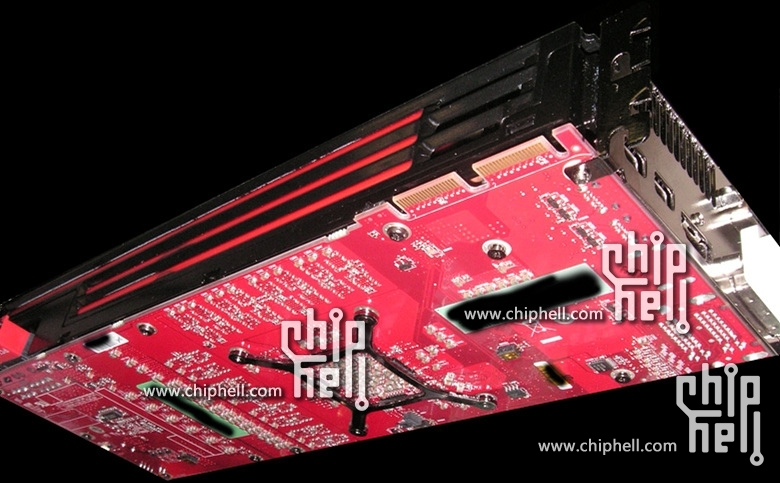
Your ass is 256bit and 48 rops?! Funny, that's what most people think the Cayman XT is going to be! 
 have you confirmed this?


 .
.

")


