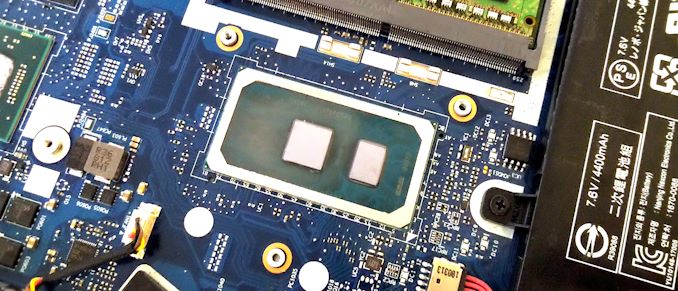
Even tho this looks like a nice shortcut the effort we put into the process is what the real value is imoIt's a lot of fun dissecting a processor. Any good enthusiast has done it once or twice I'd like to think..... I know I've done it.
Most questions have been answered, so I could only give my experience.... but meh.
I found out later down the road, you can just purchase a CPU wafer right from e-bay.

Processor Wafer for sale | eBay
Get the best deals for Processor Wafer at eBay.com. We have a great online selection at the lowest prices with Fast & Free shipping on many items!www.ebay.com
")