• Welcome to TechPowerUp Forums, Guest! Please check out our forum guidelines for info related to our community.

NVIDIA Designs New GTX 260 PCB, Further Reduces Manufacturing Costs

btarunr

Editor & Senior Moderator
Staff member
Joined
Oct 9, 2007
Messages
47,680 (7.43/day)
Location
Dublin, Ireland
System Name RBMK-1000
Processor AMD Ryzen 7 5700G
Motherboard Gigabyte B550 AORUS Elite V2
Cooling DeepCool Gammax L240 V2
Memory 2x 16GB DDR4-3200
Video Card(s) Galax RTX 4070 Ti EX
Storage Samsung 990 1TB
Display(s) BenQ 1440p 60 Hz 27-inch
Case Corsair Carbide 100R
Audio Device(s) ASUS SupremeFX S1220A
Power Supply Cooler Master MWE Gold 650W
Mouse ASUS ROG Strix Impact
Keyboard Gamdias Hermes E2
Software Windows 11 Pro
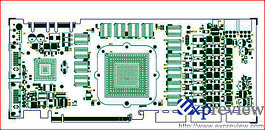
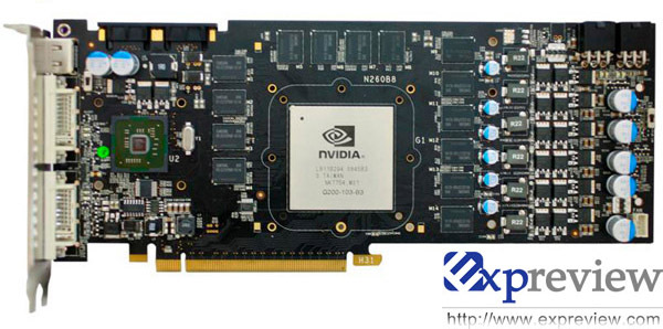
The introduction of the new G200b series graphics processors sought to revive NVIDIA's stronghold over the high-end graphics market, by reducing manufacturing costs, and facilitating high-end graphics cards at unusually low price-points, to compete with rival ATI. The first SKU using the G200b GPU was the new GeForce GTX 260. The PCB of design of the new model (P654) saw several drastic changes, that also ended up contributing to the cost-cutting: all memory chips were placed in the business end of the PCB, and the VRM area rearranged. News emerging from Expreview suggests that NVIDIA has worked out an even newer PCB reference design (model: P897) that aims mainly to cut production costs further. The reference design graphics board based on the PCB will be given the internal name "D10U-20". A short list of changes is as follows:
  • The number of PCB layers has been reduced from 10 to 8, perhaps to compress or remove blank, redundant or rudimentary connections
  • A 4+2 phase NVVDD power design using the ADP4100 voltage regulator IC, the FBVDDQ circuit has been reduced from 2 phases to 1, and the MOSFET package has been changed from LFPAK to DPAK grouping, to reduce costs. The ADP4100 lacks the I2C interface, which means voltage control will be much more difficult than on current PCBs of the GeForce 260,280, 285 and 295
  • The optional G200b support-brace has been removed
  • While the length of the PCB remains the same, the height has been reduced to cut costs
  • BIOS EEPROM capacity reduced from 1 Mbit (128 KB) to 512 Kb (64 KB)
  • Cheaper DVI connectors

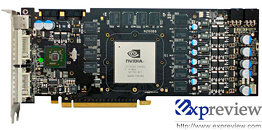
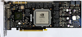
The new PCB is expected to reduce costs by as much as US $15 which will impact on the overall product cost, and help step up the competitiveness. Expreview notes that the new PCB will be available to the partners by the third week of this month. Below are the drawing and picture of the PCB. For reference, the second picture is that of the older P654 design.


View at TechPowerUp Main Site
 
Last edited:
So current gen GT200 PCB's are better then?

- Voltage Control
- Better DVI ports
- Bigger EEPROM

And do you mean width of the PCB is 1.5cm less? Got me confused for a sec cus I was thinking, "But the PCB is only about 5mm thick! :confused: ", lol.
 
It appears they are skimping out on PCB manufacturing which is not good.
 
So current gen GT200 PCB's are better then?

- Voltage Control
- Better DVI ports
- Bigger EEPROM

And do you mean width of the PCB is 1.5cm less? Got me confused for a sec cus I was thinking, "But the PCB is only about 5mm thick! :confused: ", lol.
Yes, software voltage control could get difficult as the VRM IC doesn't support the standard interface in which voltage is controlled by software. DVI ports really wouldn't make a noticeable change the older ones had EMI shielding. We doubt if the G200b made use of the extra 64 KB of EEPROM space on the older PCB. Your BIOS .rom file for the GTX260 always weighed 64KB. The "height" as in:

bta529.jpg


Look at the red line. That dimension for a PCB is called its height. For example, "half-height" cards are HTPC or Slim form-factor friendly.
 
And do you mean width of the PCB is 1.5cm less? Got me confused for a sec cus I was thinking, "But the PCB is only about 5mm thick! :confused: ", lol.

Height.
 
So current gen GT200 PCB's are better then?

- Voltage Control
- Better DVI ports
- Bigger EEPROM

And do you mean width of the PCB is 1.5cm less? Got me confused for a sec cus I was thinking, "But the PCB is only about 5mm thick! :confused: ", lol.
Its call the Height as the card is always perpendicular to the motherboard.
 
Good news post and thanks for explaining it too.
 
Which means we will get a lesser durable and lesser overclocking card, kudos to nvidia then.
 
Which means we will get a lesser durable and lesser overclocking card, kudos to nvidia then.

The only people it will hold back will be the ones trying to use software voltmod techniques. The people serious about volt modding already use the hardware method instead.

I guess some people see all news as bad news. It shouldn't make any difference except lower costs to the manufacturer and customer. Sounds like an upside.
 
sod up full cover waterblocks too id imagine?
 
The only people it will hold back will be the ones trying to use software voltmod techniques. The people serious about volt modding already use the hardware method instead.

I guess some people see all news as bad news. It shouldn't make any difference except lower costs to the manufacturer and customer. Sounds like an upside.

Maybe, but i cant see how reducing the PCB layers and VR's would not somewhat reduce the overclocking capabilities and durability.. also "cheaper" DVI connectors.. image quality degradation perhaps?
 
also "cheaper" DVI connectors.. image quality degradation perhaps?

No. All a DVI connector does is connect the card to the monitor. It's just a piece of plastic with a few sockets and metal conveying the signal. All that's different between the new one and the old, is that the old one used an EMI shield. Evidently NVIDIA found that unnecessary. Image quality is care of the NVIO2 processor. That's what handles display, and the fact that it's isolated from the GPU (and its power-hungry components) shows they've already lopped EMI, or any form of interference, although the intention of separating display logic was because the GPU die had become too big.
 
only thing i see people really complaining about is the eeprom size being shrunk, perhaps can have larger wired in.
 
I dont like it. Sounds like poorer quality all round. $15 saving on a $300-$400 card doesnt sound like its worth it.
 
I dont like it. Sounds like poorer quality all round. $15 saving on a $300-$400 card doesnt sound like its worth it.

I don't think they will pass the savings on to the consumer, this is probably so they can make more money.
 
more yields= more money to them.
 
With the global economy in such a bad shape this was to be expected. In fact they have already reduced costs with their 55nm lineup. The coolers on their 55nm lineup have been cut down. When compared to the coolers on the original 65nm GTX 260/280 lineup, the new coolers are lighter, have no back cover, heatpipes are shorter and smaller and many benchmarks reveal that in many situations 55nm parts actually run hotter than 65nm parts. Cutting down on the actual circuitry was the next logical step. They are taking the route AMD took a year ago. Hence the massive jump in Radeon 3xxx RMA's when compared to the previous generation, something that also carried on with the Radeon 4xxx lineup. In the following months you can expect a heathy increase in threads with titles such as "OMG! My brand new GTX 260 is DEAD after 2 days" or "My brand new nvidia GPU is artifacting at stock clocks!". Just watch.

Nehalem from Intel and 65nm GTX GPU's from nVidia are truly the last quality products we will see from both manufacturers since due to the worsening global economic conditions they will be cutting down on quality assurance along with everybody else in the industry. Here is an easy prediction: next massive GPU release from nVidia (384SP monster) gets pushed back by at least 6 months.
 
If it makes the card cheaper to produce, and allows the manufacturers to reduce the prices on the cards to be more competitive, this can only be seen as a good thing in the consumer's eyes.

Most consumers don't overclock the cards, and even fewer volt-mod them. So the reductions won't affect the majority of people buying the cards. And the ones that would be affected by the changes will just buy one of the more expensive versions that use the old PCB, as I'm sure both will exist side by side on the market.
 
imo this has it pros and con

pros: cheaper good nvidia cards.
cons: bad overclock, the pre-overclocked cards will have a higher DOA rate, not as durable as the first gen.

Conclusion: as long as u dont overclock, this is good, if u overclock, this is bad
 
imo this has it pros and con

pros: cheaper good nvidia cards.
cons: bad overclock, the pre-overclocked cards will have a higher DOA rate, not as durable as the first gen.

Conclusion: as long as u dont overclock, this is good, if u overclock, this is bad

Overclocking shouldn't affect durability with these changes, in fact these changes shouldn't affect durability at all unless more voltage is being run through the card(ie Volt-mods).
 
Overclocking shouldn't affect durability with these changes, in fact these changes shouldn't affect durability at all unless more voltage is being run through the card(ie Volt-mods).

+1

This is nothing but good news. The cost saving will have minimal, if any impact on the performance of the card; they are just becomeing more skilled with the manufacture of these cards and eliminating unnecessary waste.
 
Back
Top