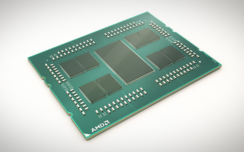
It could still be 4 cores per CCX, from
AT ~
The biggest downside from this being the insane number of
IF links to make Rome

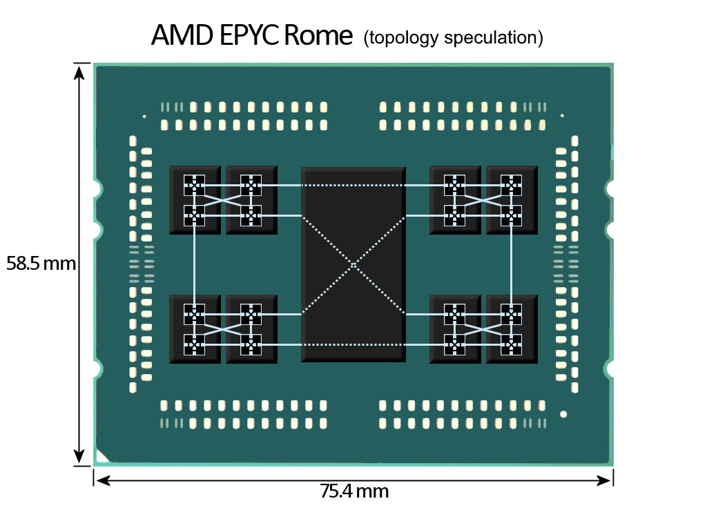
While you're right that we don't know yet that the CCXes have grown to 8 cores (though IMO this seems likely given that every other Zen2 rumor has been spot on), that drawing is ... nonsense. First off, it proposes using IF to communicate between CCXes on the same die, which even Zen1 didn't do. The sketch directly contradicts what AMD said about their design, and doesn't at all account for the I/O die and its role in inter-chiplet communication. The layout sketched out there is incredibly complicated, and wouldn't even make sense for a theoretical Zen1-based 8-die layout. Remember, IF uses PCIe links, and even in Zen1 the PCIe links were common across two CCXes. The CCXes do thus not have separate IF links, but share a common connection (through the L3 cache, IIRC) to the PCIe/IF complex. Making these separate would be a
giant step backwards in terms of design and efficiency. Remember, the uncore part of even a 2-die Threadripper consumes ~60W. And that's with two internal links, 64 lanes of PCIe and a quad-channel memory controller. The layout in the sketch above would likely consume >200W for IF alone.
Now, let's look at that sketch. In it, any given CCX is one hop away from 3-4 other CCXes, 2 hops from 3-5 CCXes, and 3 hops away from the remaining 7-10 CCXes. In comparison, with EPYC (non-Rome) and TR, all cores are 1 hop away from each other (though the inter-CCX hop is shorter/faster than the die-to-die IF hop). Even if this is "reduced latency IF" as they call it, that would be
ridiculous. And again: what role does the I/O die play in this? The IF layout in that sketch makes no use of it whatsoever, other than linking the memory controller and PCIe lanes to eight seemingly random CCXes. This would make NUMA management an impossible flustercuck on the software side, and substrate manufacturing (seriously, there are
six IF links in between each chiplet there! The chiplets are <100mm2! This is a PCB, not an interposer! You can't get that kind of trace density in a PCB.) impossible on the hardware side. Then there's the issue of this design requiring each CCX to have 4 IF links, but 1/4 of the CCXes only gets to use 3 links, wasting die area.
On the other hand, let's look at the layout that makes sense both logically, hardware and software wise, and adds up with what AMD has said about EPYC: Each chiplet has a single IF interface, that connects to the I/O die. Only that, nothing more. The I/O die has a ring bus or similar interconnect that encompasses the 8 necessary IF links for the chiplets, an additional 8 for PCIe/external IF, and the memory controllers. This reduces the number of IF links running through the substrate from 30 in your sketch (6 per chiplet pair + 6 between them) to 8. It is blatantly obvious that the I/O die has been made specifically to make this possible. This would make every single core 1 hop (through the I/O die, but ultimately still 1 hop) away from any other core, while reducing the number of IF links by almot 1/4. Why else would they design that
massive die?
Red lines. The I/O die handles low-latency shuffling of data between IF links, while also giving each chiplet "direct" access to DRAM and PCIe. All over the same single connection per chiplet. The I/O die is (at least at this time) a black box, so we don't know whether it uses some sort of ring bus, mesh topology, or large L4 cache (or some other solution) to connect these various components. But we do know that a layout like this is the only one that would actually work. (And yes, I know that my lines don't add up in terms of where the IF link is physically located on the chiplets. This is an illustration, not a technical drawing.)
More on-topic, we need to remember that IPC is workload dependent. There might be a 29% increase in IPC in certain workloads, but generally, when we talk about IPC it is
average IPC across a wide selection of workloads. This also applies when running test suites like SPEC or GeekBench, as they run a wide variety of tests stressing various parts of the core. What AMD has "presented" (it was in a footnote, it's not like they're using this for marketing) is from two specific workloads. This means that a) this can very likely be true, particularly if the workloads are FP-heavy, and b) this is very likely not representative of total average IPC across most end-user-relevant test suites. In other words, this can be both true (in the specific scenarios in question) and misleading (if read as "average IPC over a broad range of workloads").


 ?
?
")
