Common sense dictates Polaris should have been 1500 MHz too but it launched at 1266 MHz. The most similar chip to Vega is Fiji which launched at 1050 MHz.
Source?
Edit: working backwards from the
numbers here you'd need 1525 MHz to get 12.5 TFLOP.
Imma let you finish but...
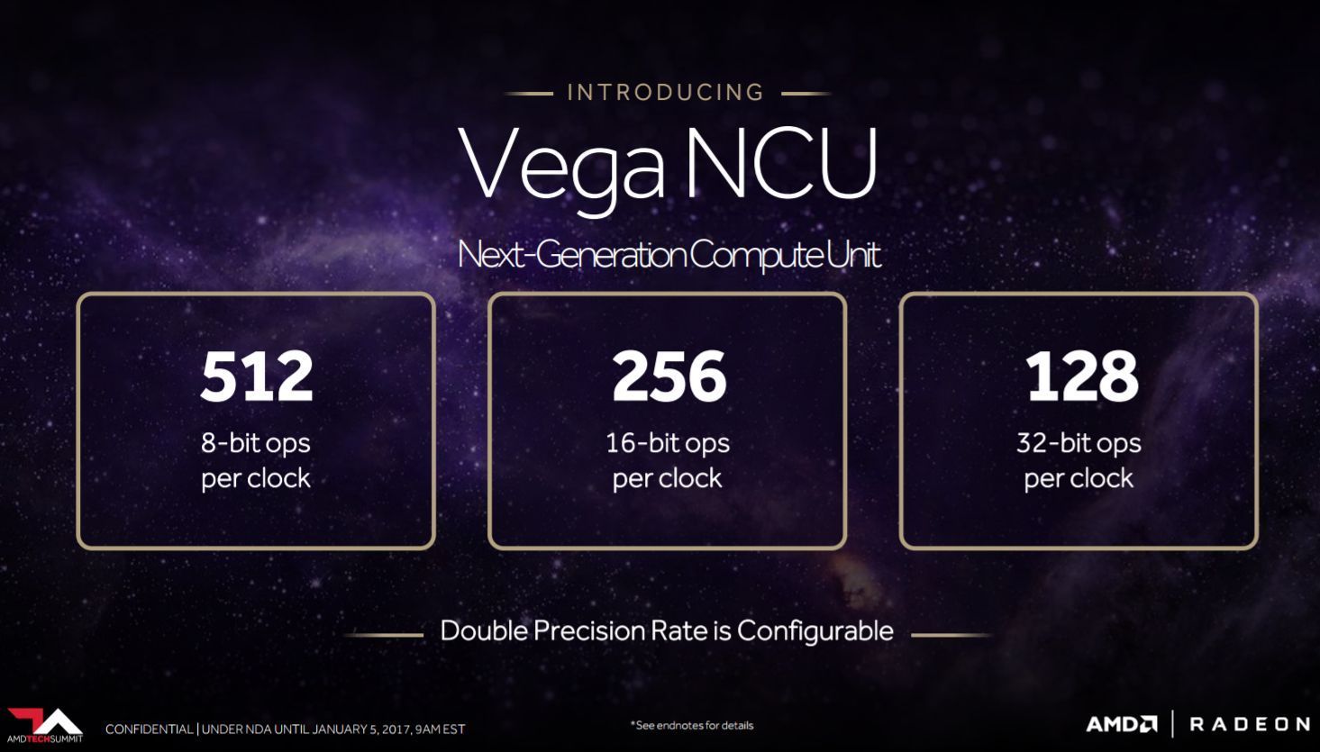
-12.5 TFLOP is derived from the
Vega Cube (quad Vega, ~50 TFLOP).
-Titan Xp is
also 12 TFLOP.
-Before you get all excited about the above, RX 480 is
5.8 TFLOP (215%) while RX 580 is
6.2 TFLOP (202%).
-AMD takes about a 30% TFLOP hit when doing games compared to NVIDIA (RX 580 should match GTX 1070 according to TFLOPs but it doesn't).
1) The 380X was clocked at 1030 MHz, and thus Fiji was clocked
higher than it's lower-tier brethren. I can do this all day:
-7850 was clocked lower than the 7970.
-The 6800 series clocked almost exactly the same as the 6900 series
-7790 was clocked the same as the 290X
The fact is there is absolutely no consistent pattern of AMD clocking their higher-end cards lower than their smaller cards. None.
It is Nvidia that has a tendency to clock the top cards slower, not AMD.
2) "you'd need 1525 MHz to get 12.5 TFLOP."
Yes.
3) "AMD takes about a 30% TFLOP hit when doing games compared to NVIDIA"
Nope, Polaris does. We don't know what Vega's FPS/flops ratio is yet. But we do know this is the biggest architectural shift AMD has made in 6 years, and we also know AMD is switching to tiled rendering like Nvidia did with Maxwell. Thus it is not crazy to think AMD will come close to Nvidia's TFLOPS efficiency, but again
we don't know yet!
AMD's
confirmed professional version of Vega cards have
over double the stats of the 480, and let's see how that would stack up:
^Hmmm right next to a 1080 Ti, and that is
before ANY architectural enhancements are considered.
")

