- Joined
- Oct 9, 2007
- Messages
- 47,680 (7.43/day)
- Location
- Dublin, Ireland
| System Name | RBMK-1000 |
|---|---|
| Processor | AMD Ryzen 7 5700G |
| Motherboard | Gigabyte B550 AORUS Elite V2 |
| Cooling | DeepCool Gammax L240 V2 |
| Memory | 2x 16GB DDR4-3200 |
| Video Card(s) | Galax RTX 4070 Ti EX |
| Storage | Samsung 990 1TB |
| Display(s) | BenQ 1440p 60 Hz 27-inch |
| Case | Corsair Carbide 100R |
| Audio Device(s) | ASUS SupremeFX S1220A |
| Power Supply | Cooler Master MWE Gold 650W |
| Mouse | ASUS ROG Strix Impact |
| Keyboard | Gamdias Hermes E2 |
| Software | Windows 11 Pro |
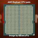
We've known since last week that AMD's upcoming desktop processor socket, AM5, will be a land-grid array (LGA), much like Intel's desktop sockets; and today we have a first-look at what the land-grid will look like, courtesy of ExecutableFix, who first broke news of AM5 being an LGA of 1,718 pins. Below is a render of the AM5 contact pad (the underside of the processor). The 1,718 contacts span across the fiberglass substrate, with no socket island in the middle for ancillaries. All electrical ancillaries are located on the obverse side of the substrate, surrounding the die(s). The substrate area will remain 40 mm x 40 mm, so the processor package will be roughly of the same size as AM4. In comparison, Intel's upcoming LGA1700 package is expected to measure 37.5 mm x 45 mm (a rectangular substrate).
ExecutableFix put out a handful more details about the I/O of this socket. Apparently, AM5 is a pure-DDR5 platform, with no backwards compatibility with DDR4. The socket features a dual-channel DDR5 memory interface. The PCI-Express interface is PCI-Express 4.0, with the socket putting out 28 lanes in total. 16 of these go to the PEG slot(s), four to an M.2 NVMe slot, and possibly the remaining eight as chipset bus. Considering these are Gen 4, the next-generation X670 (X570 successor) chipset could have double the chipset-bus bandwidth compared to Intel Z590. A typical Socket AM5 chip, such as "Rembrandt," could feature a TDP of 120 W, going up to 170 W, according to the source.
View at TechPowerUp Main Site
ExecutableFix put out a handful more details about the I/O of this socket. Apparently, AM5 is a pure-DDR5 platform, with no backwards compatibility with DDR4. The socket features a dual-channel DDR5 memory interface. The PCI-Express interface is PCI-Express 4.0, with the socket putting out 28 lanes in total. 16 of these go to the PEG slot(s), four to an M.2 NVMe slot, and possibly the remaining eight as chipset bus. Considering these are Gen 4, the next-generation X670 (X570 successor) chipset could have double the chipset-bus bandwidth compared to Intel Z590. A typical Socket AM5 chip, such as "Rembrandt," could feature a TDP of 120 W, going up to 170 W, according to the source.

View at TechPowerUp Main Site


