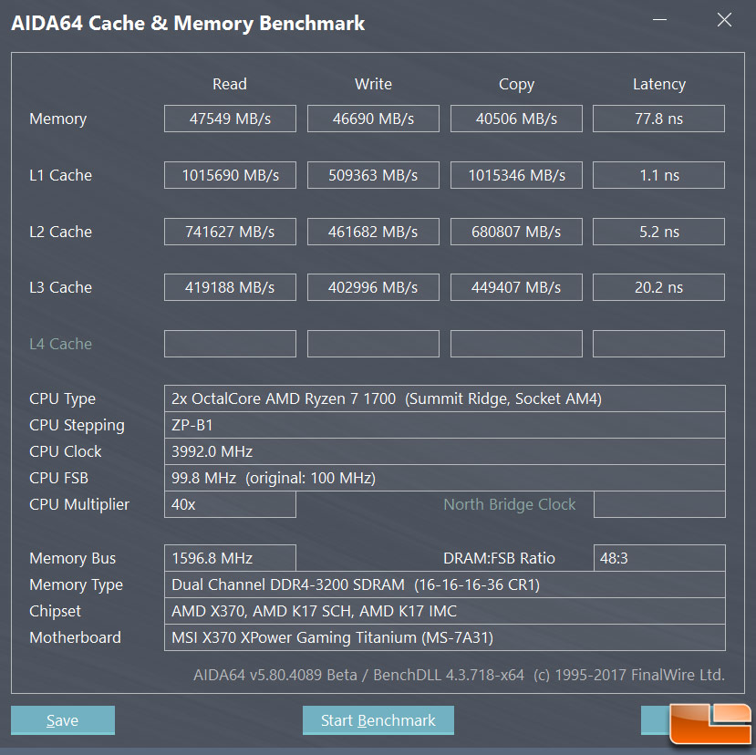
The cache design of Ryzen 7 suggests that an even better way to handle it would be to schedule it as a two socket system, each of which is a 4c 8t CPU. The L3 cache is divided into two parts, and performance is much worse if a core on side A needs data from side B or vice versa.
What an interesting suggestion.
Your paradigm of splitting, for coding purposes, the 8 cores into discrete 4 core ccxS & 8MB L3 cache blocks. & then minimising interaction between them, could speed some apps considerably.
I am a newb~, but i mused similarly in the context of a poor mans vega pro ssg (a 16GB $5000+ Vega w/ an onboard 4x 960 pro raid array).
if you install an Affordable 8 lane vega and an 8 lane 2x nvme adapter, so both link to the same 16 lane ccx (as a 16 lane card does e.g.) , then the gpu and the 2x nvme raid array may be able to talk very directly, and ~share the same 8MB cpu L3 cache. It doesnt bypass the shared pcie bus like Vega SSG, but it could be minimal latency, and enhanced by specialised large block size formatting for; swapping, workspace, temp files and graphics.
Vega 56/64 of course, have a dedicated HBCC subsystem for such gpu cache extension using nvme arrays. Done right, it promises a pretty good illusion of ~unlimited gpu memory/address space. Cool indeed.
As you see, a belated post from me. We now have evidence in the perf figures of single ccx zen/vega apuS. Yes, inter ccx interconnects have dragged Ryzen ~IPC down.


")