• Welcome to TechPowerUp Forums, Guest! Please check out our forum guidelines for info related to our community.

Samsung to Optical-Shrink NVIDIA "Pascal" to 14 nm

btarunr

Editor & Senior Moderator
Staff member
Joined
Oct 9, 2007
Messages
47,670 (7.43/day)
Location
Dublin, Ireland
System Name RBMK-1000
Processor AMD Ryzen 7 5700G
Motherboard Gigabyte B550 AORUS Elite V2
Cooling DeepCool Gammax L240 V2
Memory 2x 16GB DDR4-3200
Video Card(s) Galax RTX 4070 Ti EX
Storage Samsung 990 1TB
Display(s) BenQ 1440p 60 Hz 27-inch
Case Corsair Carbide 100R
Audio Device(s) ASUS SupremeFX S1220A
Power Supply Cooler Master MWE Gold 650W
Mouse ASUS ROG Strix Impact
Keyboard Gamdias Hermes E2
Software Windows 11 Pro
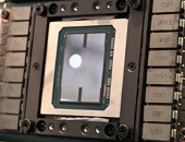
It looks like NVIDIA won't skip the 14 nm process en route sub-10 nm nodes, despite meeting its energy-efficiency targets with the 16 nm FinFET node, after all. The company has reportedly concluded talks with Samsung Electronics, to optically-shrink its current GeForce "Pascal" architecture down to the newer 14 nanometer FinFET node, by Samsung. It's unclear as to whether specific upcoming (unreleased) Pascal GPUs will get 14 nm treatment, or if this is a series-wide die-shrink of the kind NVIDIA did between the 65 nm and 55 nm nodes. The Samsung-made 14 nm "Pascal" GPUs should enter production before year-end.


View at TechPowerUp Main Site
 
I think they'll wait for a refresh of the series...
 
Ti most likely. Probably GTX 1060Ti and 1080Ti. Similar to how they've done it in the past.
 
GTX 1080+ anyone? :laugh:

throwback to 9800 GTX and 9800GTX+
 
Shrinking the GTX 1080 to 250 sq.mm GTX 1160 more likely. GTX 1060 can't be shrink-ed without dropping the 192 bit. The 1170/1180 could be the shrink of pascal titan on 256 bit.
 
Haven't we seen this kinda before with Samsung doing some work then TSMC does it better like for Apple's iphone the TSMC made chip was faster then Samsung? o_O
 
Does not make much sense, 14nm lpp and 16nm FF+ are quite the same size. There's not much die size savings on that shrink. Maybe they will make pascal tegras on samsungs 14nm LPP, but I don't see them moving their whole gpu line from TSMC. Maybe they try something like gp107 or gp108 on samsungs manufacturing nodes...
 
This is great news. I love reading something like this.
Samsung's phenomenal line, i thought were preserved for AMD only.
 
sounds more like a trial&error run
 
OMFG SATURDAY NEWS! YES!!

This is like Saturday morning cartoons for us!

I love that picture too.... That's what it looks like inside the Terminator's brain!
 
Makes me wonder if TSMC is having yield problems on 16nm like they did when they went from 40nm to 28nm. That could in part explain the shortages but I think most of the shortage of 1070 and 1080 is due to their extremely good performance and a lot of people want them. Maybe Nvidia is finally fed up with TSMC.
 
Most probably for GP100. It makes sense to reduce the power consumption as large quantities of GP100 is expected to be used with upcoming Power 9 servers.
 
Probably mobile Tegra chips based on Pascal architecture. Why would you try making high power chips on low power Samsung/GloFo 14nm finfet process like AMD did.
 
Now that die shrinks are getting ever harder, I'm not surprised that they are taking this step.

If I remember correctly, at around 3-7nm you reach the size of single atoms, so we're close to the limit now.
 
Now that die shrinks are getting ever harder, I'm not surprised that they are taking this step.

If I remember correctly, at around 3-7nm you reach the size of single atoms, so we're close to the limit now.

No, atoms are much smaller that that.

http://hyperphysics.phy-astr.gsu.edu/hbase/particles/atomsiz.html

But the lower process nodes are introducing more difficulties.

Probably new materials other than silicon will help.

http://arstechnica.com/gadgets/2015...d-to-10nm-will-move-away-from-silicon-at-7nm/
 
Probably outcome of Samsung bringing nvidia to knees. Also it seems like when it comes to fab Samsung is now ruling the roost.
 
Seems like an TSMC supply issue, it will be interesting to see what happens to the power consumption.
 
Shrinking the GTX 1080 to 250 sq.mm GTX 1160 more likely. GTX 1060 can't be shrink-ed without dropping the 192 bit. The 1170/1180 could be the shrink of pascal titan on 256 bit.

While it does look that way, I find it extremely unlikely they'll go under 280mm². Sure, the name says 14nm, but a lot of the die isn't at 14nm (some smaller, like a fin on 22nm Intel FinFET being a mere 8nm wide, or a channel length of 28nm, on the very same node). You can read more about how node sizes have become essentially marketing here http://spectrum.ieee.org/semiconductors/devices/the-status-of-moores-law-its-complicated

Haven't we seen this kinda before with Samsung doing some work then TSMC does it better like for Apple's iphone the TSMC made chip was faster then Samsung? o_O

Probably outcome of Samsung bringing nvidia to knees. Also it seems like when it comes to fab Samsung is now ruling the roost.

Err.. wat? nV and Samsung don't compete against each other in any market besides SoCs (Tegra vs Exynos). Ans for best fab, that would arguably be Intel who are on their second generation of FinFETs, with extra tweaks beyond what was done with the first 14nm chips.

Seems like an TSMC supply issue, it will be interesting to see what happens to the power consumption.

That was my first thought as well.

Probably mobile Tegra chips based on Pascal architecture. Why would you try making high power chips on low power Samsung/GloFo 14nm finfet process like AMD did.

Possible, but you can do some very interesting custom tweaks to your chips to let them clock really high even on the same node (mostly because at this point the limiter on clock speeds is either chip layout (literally where the transistors are and how they're wired), or much more commonly these days, power), or lower power on the same node. Just compare Tonga vs Tahiti (R9-285 vs R9-280 in particular), or Fermi GF100 vs GF110 (GTX 480 vs GTX 570 in particular), both of which both lowered power (measurably so in both cases.. according to AnandTech at least) and increased performance through higher clockspeeds and/or fewer disabled clusters on higher-power SKUs.
 
Shrinking the GTX 1080 to 250 sq.mm GTX 1160 more likely. GTX 1060 can't be shrink-ed without dropping the 192 bit. The 1170/1180 could be the shrink of pascal titan on 256 bit.

What are you talking about? They can shrink the die and keep the bus size.
 
Does not make much sense, 14nm lpp and 16nm FF+ are quite the same size. There's not much die size savings on that shrink. Maybe they will make pascal tegras on samsungs 14nm LPP, but I don't see them moving their whole gpu line from TSMC. Maybe they try something like gp107 or gp108 on samsungs manufacturing nodes...
Exactly what I think this move is to mean. Cost/chip might be another factor for nVidia desicion. Capacity a 3rd one. Who knows? All will be clear once we learn the products of the collaboration.
 
Based on that picture it looks like a mobile chip.
 
Back
Top