Report an Error


ATI Rage PRO
Rage PRO

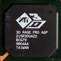
3D Rage PRO AGP

3D Rage PRO PCI

Fritzchens Fritz
Die Shot
ATI's Rage PRO GPU uses the Rage 3 architecture and is made using a 350 nm production process at UMC. With a die size of 47 mm² and a transistor count of 8 million it is a very small chip. Rage PRO supports DirectX 6.0. Modern GPU compute technologies are not available. It features 1 pixel shaders and 0 vertex shaders, 1 texture mapping units and 1 ROPs. Due to the lack of unified shaders you will not be able to run recent games at all (which require unified shader/DX10+ support).
Graphics Processor
- Released
- Mar 1st, 1997
- GPU Name
- Rage PRO
- Architecture
- Rage 3
- Foundry
- UMC
- Process Size
- 350 nm
- Transistors
- 8 million
- Density
- 170.2K / mm²
- Die Size
- 47 mm²
Graphics Features
- DirectX
- 6.0
- OpenGL
- 1.1
- OpenCL
- N/A
- Vulkan
- N/A
- Pixel Shader
- N/A
- Vertex Shader
- N/A
Render Config
- Pixel Shaders
- 1
- Vertex Shaders
- 0
- TMUs
- 1
- ROPs
- 1
All Rage 3 GPUs
- ATI Rage PRO
- ATI Rage PRO Turbo
- ATI Rage XL
ATI GPU Architecture History
Graphics cards using the ATI Rage PRO GPU
| Name | Chip | Memory | Shaders | TMUs | ROPs | GPU Clock | Memory Clock |
|---|---|---|---|---|---|---|---|
| 3D Rage PRO AGP | 2 MB | 1 / 0 | 1 | 1 | 75 MHz | 75 MHz | |
| 3D Rage PRO PCI | 8 MB | 1 / 0 | 1 | 1 | 75 MHz | 75 MHz |


Apr 26th, 2024 13:40 EDT
change timezone
Latest GPU Drivers
New Forum Posts
- DTS:X APO4 + DTS Interactive for Most Devices [USB Supported] (305)
- The Official Linux/Unix Desktop Screenshots Megathread (702)
- What's your latest tech purchase? (20352)
- hacked (73)
- im new to throttelstop and i think i messed it up by copying others any hints would be very much aprreciated (5)
- 2022-X58/1366 PIN Motherboards NVME M.2 SSD BIOS MOD Collection (657)
- DTS DCH Driver for Realtek HDA [DTS:X APO4 + DTS Interactive] (1909)
- checkup (1)
- Help me to OC my 5700X (10)
- XFX RX470 8GB no video and error 43 (28)
Popular Reviews
- HYTE THICC Q60 240 mm AIO Review
- MOONDROP x Crinacle DUSK In-Ear Monitors Review - The Last 5%
- Alienware Pro Wireless Gaming Keyboard Review
- Upcoming Hardware Launches 2023 (Updated Feb 2024)
- Logitech G Pro X Superlight 2 Review - Updated with 4000 Hz Tested
- Thermalright Phantom Spirit 120 EVO Review
- AMD Ryzen 5 7600 Review - Affordable Zen 4 for the Masses
- FiiO K19 Desktop DAC/Headphone Amplifier Review
- ASUS Radeon RX 7900 GRE TUF OC Review
- RTX 4090 & 53 Games: Ryzen 7 5800X vs Ryzen 7 5800X3D Review
Controversial News Posts
- Windows 11 Now Officially Adware as Microsoft Embeds Ads in the Start Menu (128)
- Sony PlayStation 5 Pro Specifications Confirmed, Console Arrives Before Holidays (117)
- NVIDIA Points Intel Raptor Lake CPU Users to Get Help from Intel Amid System Instability Issues (106)
- AMD "Strix Halo" Zen 5 Mobile Processor Pictured: Chiplet-based, Uses 256-bit LPDDR5X (102)
- US Government Wants Nuclear Plants to Offload AI Data Center Expansion (98)
- AMD's RDNA 4 GPUs Could Stick with 18 Gbps GDDR6 Memory (92)
- Developers of Outpost Infinity Siege Recommend Underclocking i9-13900K and i9-14900K for Stability on Machines with RTX 4090 (85)
- Windows 10 Security Updates to Cost $61 After 2025, $427 by 2028 (84)