Report an Error


NVIDIA C89

MCP89UL-A3

MCP89UZ-A3
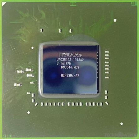
MCP89MZ-A2

MCP89MZ-A3

TPC Diagram
NVIDIA's C89 GPU uses the Tesla 2.0 architecture and is made using a 40 nm production process. With a die size of 100 mm² and a transistor count of 486 million it is a small chip. C89 supports DirectX 11.1 (Feature Level 10_1). For GPU compute applications, OpenCL version N/A can be used. It features 48 shading units, 16 texture mapping units and 8 ROPs.
Further reading:
Tesla Architecture Whitepaper 
Graphics Processor
- Released
- Apr 1st, 2010
- GPU Name
- C89
- Codename
- NVAF
- Architecture
- Tesla 2.0
- Process Size
- 40 nm
- Transistors
- 486 million
- Density
- 4.9M / mm²
- Die Size
- 100 mm²
Graphics Features
- DirectX
- 11.1 (10_1)
- OpenGL
- 3.3
- OpenCL
- N/A
- Vulkan
- N/A
- Shader Model
- 4.1
- WDDM
- 1.2
- PureVideo HD
- VP4
- VDPAU
- Feature Set C
Render Config
- Shading Units
- 48
- TMUs
- 16
- ROPs
- 8
- SM Count
- 4
- SFUs
- 12
- TPCs
- 3
- Tex L1 Cache
- 16 KB per TPC
- Max. TDP
- 23 W
All Tesla 2.0 GPUs
NVIDIA GPU Architecture History
- 2024 Blackwell
- 2023 Hopper
- 2022-2024 Ada Lovelace
- 2020-2024 Ampere
- 2018-2022 Turing
- 2017-2020 Volta
- 2016-2021 Pascal
- 2014-2019 Maxwell 2.0
- 2014-2017 Maxwell
- 2013-2015 Kepler 2.0
- 2012-2018 Kepler
- 2010-2016 Fermi 2.0
- 2010-2013 VLIW Vec4
- 2010-2016 Fermi
- 2007-2013 Tesla 2.0
- 2006-2010 Tesla
- 2003-2013 Curie
- 2003-2005 Rankine
- 2001-2003 Kelvin
- 1999-2005 Celsius
- 1998-2000 Fahrenheit
Graphics cards using the NVIDIA C89 GPU
| Name | Chip | Memory | Shaders | TMUs | ROPs | GPU Clock | Memory Clock |
|---|---|---|---|---|---|---|---|
| MCP89UL-A3 | System Shared | 48 | 16 | 8 | 450 MHz | System Shared |
C89 GPU Notes
| PureVideo HD: VP4 VDPAU: Feature Set C |
Apr 26th, 2024 17:49 EDT
change timezone
Latest GPU Drivers
New Forum Posts
- looking to build a new system and im considering asrock brand but i have some doubts/concerns. (5)
- TPU's Nostalgic Hardware Club (18474)
- What's your latest tech purchase? (20354)
- 5800x (and other Zen 3 chips) PBO settings/Temperature fix (934)
- Only EDP Other in Core? (2)
- Alphacool CORE 1 CPU block - bulging with danger of splitting? (30)
- Dell Workstation Owners Club (3061)
- Xeon Owners Club (8700)
- Secure boot already open help (10)
- hacked (77)
Popular Reviews
- HYTE THICC Q60 240 mm AIO Review
- MOONDROP x Crinacle DUSK In-Ear Monitors Review - The Last 5%
- Upcoming Hardware Launches 2023 (Updated Feb 2024)
- Alienware Pro Wireless Gaming Keyboard Review
- Thermalright Phantom Spirit 120 EVO Review
- FiiO K19 Desktop DAC/Headphone Amplifier Review
- ASUS Radeon RX 7900 GRE TUF OC Review
- Ugreen NASync DXP4800 Plus Review
- AMD Ryzen 7 7800X3D Review - The Best Gaming CPU
- Sapphire Radeon RX 7900 GRE Pulse Review
Controversial News Posts
- Windows 11 Now Officially Adware as Microsoft Embeds Ads in the Start Menu (135)
- Sony PlayStation 5 Pro Specifications Confirmed, Console Arrives Before Holidays (117)
- NVIDIA Points Intel Raptor Lake CPU Users to Get Help from Intel Amid System Instability Issues (106)
- AMD "Strix Halo" Zen 5 Mobile Processor Pictured: Chiplet-based, Uses 256-bit LPDDR5X (103)
- US Government Wants Nuclear Plants to Offload AI Data Center Expansion (98)
- AMD's RDNA 4 GPUs Could Stick with 18 Gbps GDDR6 Memory (95)
- Developers of Outpost Infinity Siege Recommend Underclocking i9-13900K and i9-14900K for Stability on Machines with RTX 4090 (85)
- Windows 10 Security Updates to Cost $61 After 2025, $427 by 2028 (84)