Report an Error


NVIDIA Playstation 3 GPU 90nm
- Graphics Processor
- RSX-90nm
- Pixel Shaders
- 24
- Vertex Shaders
- 8
- TMUs
- 24
- ROPs
- 8
- Memory Size
- 256 MB
- Memory Type
- GDDR3
- Bus Width
- 128 bit

GPU

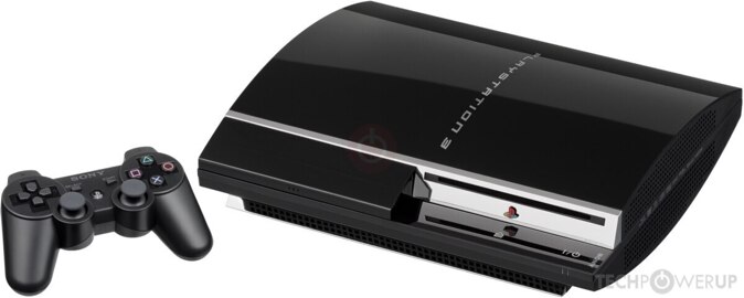
Front 2
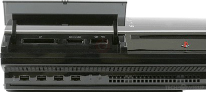
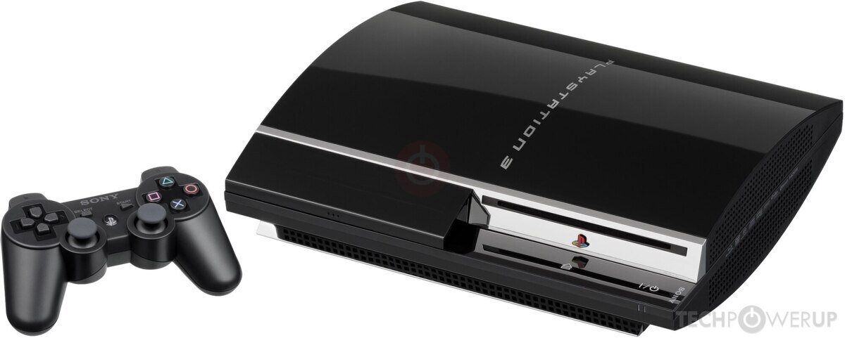
Front 3
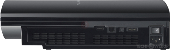
Back
Recommended Gaming Resolutions:
- 640x480
- 1280x720
- 1366x768
The Playstation 3 GPU 90nm was a high-end gaming console graphics solution by NVIDIA, launched on November 11th, 2006. Built on the 90 nm process, and based on the RSX-90nm graphics processor, in its RSX-CXD2971 variant, the device does not support DirectX. The RSX-90nm graphics processor is an average sized chip with a die area of 258 mm² and 300 million transistors. It features 24 pixel shaders and 8 vertex shaders, 24 texture mapping units, and 8 ROPs. NVIDIA includes 256 MB GDDR3 memory, which are connected using a 128-bit memory interface. The GPU is operating at a frequency of 550 MHz, memory is running at 650 MHz.
Its power draw is rated at 80 W maximum. The console's dimensions are 325 mm x 98 mm x 274 mm, and it features a igp cooling solution. Its price at launch was 599 US Dollars.
Its power draw is rated at 80 W maximum. The console's dimensions are 325 mm x 98 mm x 274 mm, and it features a igp cooling solution. Its price at launch was 599 US Dollars.
Graphics Processor
Graphics Card
- Release Date
- Nov 11th, 2006
- Generation
-
Console GPU
(Sony)
- Production
- End-of-life
- Launch Price
- 599 USD
Clock Speeds
- GPU Clock
- 550 MHz
- Memory Clock
-
650 MHz
1300 Mbps effective
Memory
- Memory Size
- 256 MB
- Memory Type
- GDDR3
- Memory Bus
- 128 bit
- Bandwidth
- 20.80 GB/s
Render Config
- Pixel Shaders
- 24
- Vertex Shaders
- 8
- TMUs
- 24
- ROPs
- 8
Theoretical Performance
- Pixel Rate
- 4.400 GPixel/s
- Vertex Rate
- 1.100 GVertices/s
- Texture Rate
- 13.20 GTexel/s
Board Design
- Length
- 325 mm
12.8 inches
- Width
- 98 mm
3.9 inches
- Height
- 274 mm
10.8 inches
- Weight
- 5.0 kg (11.0 lbs)
- TDP
- 80 W
- Outputs
- 1x HDMI 1.3
Graphics Features
- DirectX
- N/A
- OpenGL
- ES 1.1
- OpenCL
- N/A
- Vulkan
- N/A
- Pixel Shader
- 3.0
- Vertex Shader
- 3.0
Console Notes
| Playstation 3 (1st Generation) 60GB CECHAxx = November 11th, 2006 20GB CECHBxx = November 11th, 2006 Playstation 3 (2nd Generation) 60GB CECHCxx = March 23rd, 2007 80GB CECHExx = August, 2007 Playstation 3 (3rd Generation) 40GB CECHGxx = October, 2007 40GB CECHHxx = October, 2007 |
RSX-90nm GPU Notes
| Multi-way programmable parallel floating-point shader pipelines Independent pixel/vertex shader architecture 24 parallel pixel-shader ALU pipes clocked @ 550 MHz 5 ALU operations per pipeline, per cycle - 2 vector4 - 2 scalar/dual/co-issue and fog ALU - 1 Texture ALU 16 floating-point operations per pipeline, per cycle Pixel Floating Point Operations: 211.2 GFLOPS (550MHz x 24 Shaders x 16 ops per clock per cycle) 8 parallel vertex pipelines @ 500 MHz 2 ALU operations per pipeline, per cycle - 1 vector4 - 1 scalar, dual issue 10 floating-point operations per pipeline, per cycle Vertex Floating Point Operations: 40.0 GFLOPS (500MHz x 8 Shaders x 10 ops per clock per cycle) Total Floating Point Operations: 251.2 GFLOPS (550MHz x 24 Shaders x 16 ops per clock per cycle) +(500MHz x 8 Shaders x 10 ops per clock per cycle) 74.0 billion shader operations/s (24 Pixel Shader Pipelines x 5 ALUs x 550 MHz) +(8 Vertex Shader Pipelines x 2 ALUs x 500 MHz) 24 texture filtering units (TF) 8 vertex texture addressing units (TA) 24 filtered samples per clock Peak texel fillrate: 13.2 GTexel/s (24 textures x 550 MHz) 32 unfiltered texture samples per clock (8 TA x 4 texture samples) 8 Render Output units / pixel rendering pipelines Peak pixel fillrate: 4.4 GPixel/s (8 ROPs x 550 MHz) Peak Z sample rate: 8.8 GSamples/s (2 Z-samples x 8 ROPs x 550 MHz) Peak Dot product operations: 56 billion/s (combined with Cell CPU) 128-bit pixel precision offers rendering of scenes with High dynamic range rendering (HDR) Cell FlexIO bus interface 20 GB/s read to the Cell and XDR memory 15 GB/s write to the Cell and XDR memory Support for PSGL (OpenGL ES 1.1 + Nvidia Cg) Support for S3TC texture compression |
May 8th, 2024 01:39 EDT
change timezone
Latest GPU Drivers
New Forum Posts
- Does anyone here overclock their video cards? Is it really worth it? (16)
- Download Windows 10/11 ESD (1061)
- GPU Hot Spot Temperature 105 Celsius, fans at 3000 RPM, while GPU Temperature is max 70 Celsius (43)
- POLL: Can you see the difference past 60fps (gaming/other) (17)
- Steam Deck Owners Clubhouse (389)
- What are you playing? (20600)
- What's your latest tech purchase? (20474)
- Arc OC'ing, anyone? (4)
- Silly question about upcoming CPU Upgrade (10)
- 6800XT Red Devil with 18°C difference from Core to Hotspot (9)
Popular Reviews
- CHERRY XTRFY M64 Pro Review
- Corsair iCUE Link RX120 RGB 120 mm Fan Review
- Finalmouse UltralightX Review
- Cougar Hotrod Royal Gaming Chair Review
- Upcoming Hardware Launches 2023 (Updated Feb 2024)
- Meze Audio LIRIC 2nd Generation Closed-Back Headphones Review
- AMD Ryzen 7 7800X3D Review - The Best Gaming CPU
- ASRock NUC BOX-155H (Intel Core Ultra 7 155H) Review
- ASUS Radeon RX 7900 GRE TUF OC Review
- Sapphire Radeon RX 7900 GRE Pulse Review
Controversial News Posts
- Intel Statement on Stability Issues: "Motherboard Makers to Blame" (258)
- AMD to Redesign Ray Tracing Hardware on RDNA 4 (201)
- Windows 11 Now Officially Adware as Microsoft Embeds Ads in the Start Menu (167)
- NVIDIA to Only Launch the Flagship GeForce RTX 5090 in 2024, Rest of the Series in 2025 (133)
- Sony PlayStation 5 Pro Specifications Confirmed, Console Arrives Before Holidays (119)
- AMD's RDNA 4 GPUs Could Stick with 18 Gbps GDDR6 Memory (114)
- NVIDIA Points Intel Raptor Lake CPU Users to Get Help from Intel Amid System Instability Issues (106)
- AMD Ryzen 9 7900X3D Now at a Mouth-watering $329 (104)