Report an Error


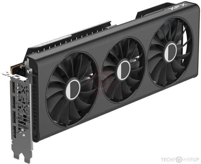
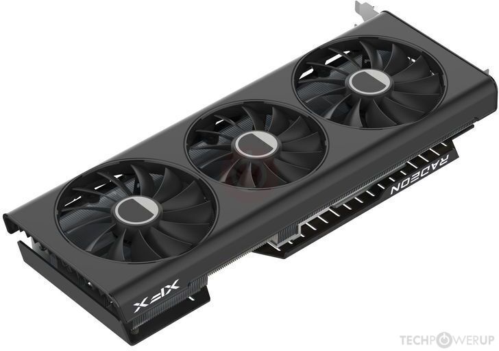
XFX RX 7900 GRE
- RX-79GMERCBR
- Graphics Processor
- Navi 31
- Cores
- 5120
- TMUs
- 320
- ROPs
- 160
- Memory Size
- 16 GB
- Memory Type
- GDDR6
- Bus Width
- 256 bit

GPU
Top

Back
Graphics Processor
- GPU Name
- Navi 31
- Codename
- Plum Bonito
- GPU Variant
-
Navi 31 XL
(215-145000206)
- Architecture
- RDNA 3.0
- Foundry
- TSMC
- Process Size
- 5 nm
- MCD Process
- 6 nm
- Process Type
- N5 / N6 FinFET
- Transistors
- 57,700 million
- GCD Transistors
- 45,400 million
- MCD Transistors
- 2,050 million x6
- Density
- 109.1M / mm²
- GCD Density
- 150.2M / mm²
- MCD Density
- 54.64M / mm²
- Die Size
- 529 mm²
- GCD Die Size
- 304.35 mm²
- MCD Die Size
- 37.52 mm² x6
- Chip Package
- MCM
Graphics Card
Clock Speeds
- Base Clock
1287 MHz
1681 MHz (+31%)
- Shader Clock
1880 MHz
2052 MHz (+9%)
- Game Clock
1880 MHz
2052 MHz (+9%)
- Boost Clock
2245 MHz
2391 MHz (+7%)
- Memory Clock
-
2250 MHz
18 Gbps effective
Memory
- Memory Size
- 16 GB
- Memory Type
- GDDR6
- Memory Bus
- 256 bit
- Bandwidth
- 576.0 GB/s
Render Config
- Shading Units
- 5120
- TMUs
- 320
- ROPs
- 160
- Compute Units
- 80
- RT Cores
- 80
- L0 Cache
- 64 KB per WGP
- L1 Cache
- 256 KB per Array
- L2 Cache
- 6 MB
- L3 Cache
- 64 MB
Theoretical Performance
- Pixel Rate
-
359.2 GPixel/s
382.6 GPixel/s
- Texture Rate
-
718.4 GTexel/s
765.1 GTexel/s
- FP16 (half)
-
91.96 TFLOPS
97.94 TFLOPS (2:1)
- FP32 (float)
-
45.98 TFLOPS
48.97 TFLOPS
- FP64 (double)
-
1,437 GFLOPS
1.530 TFLOPS (1:32)
Board Design
- Slot Width
Dual-slot
Triple-slot
- Length
276 mm
335 mm
10.9 inches
13.2 inches
- Width
110 mm
130 mm
4.3 inches
5.1 inches
- TDP
- 260 W
- Suggested PSU
- 600 W
- Outputs
- 1x HDMI 2.1a
2x DisplayPort 2.1
1x USB Type-C
- Power Connectors
- 2x 8-pin
- Board Number
- 109-D712A7-00_02
Graphics Features
- DirectX
- 12 Ultimate (12_2)
- OpenGL
- 4.6
- OpenCL
- 2.2
- Vulkan
- 1.3
- Shader Model
- 6.7
Navi 31 GPU Notes
| Generation: Navi III Codename: Plum Bonito Ray Tracing Cores: 2nd Gen Infinity Cache: 2nd Gen Graphics/Compute: 11.0.0 Shader ISA: GFX11.0 (gfx1100) Display Core Next: 3.2.0 Video Core Next: 4.0.0 System DMA: 6.0.0 Per SIMD32: - 10 KB Scalar Register File Per CU: - 16 KB Vector Data Cache - 64 KB Local Data Share (GCN-Mode) Per WGP: - 16 KB Scalar Data Cache / K Cache - 32 KB Instruction Cache - 128 KB Local Data Share |
Other retail boards based on this design (13)
| Name | GPU Clock | Boost Clock | Memory Clock | Other Changes |
|---|---|---|---|---|
| 1358 MHz | 2293 MHz | 2250 MHz | Triple-slot | |
| 1448 MHz | 2333 MHz | 2250 MHz | Triple-slot | |
| 1448 MHz | 2333 MHz | 2250 MHz | 320 mm/12.6 inches, Triple-slot | |
| 1448 MHz | 2333 MHz | 2250 MHz | 320 mm/12.6 inches, Triple-slot | |
| 1681 MHz | 2391 MHz | 2250 MHz | 302 mm/11.9 inches, Triple-slot | |
| 1358 MHz | 2293 MHz | 2250 MHz | 290 mm/11.4 inches | |
| 1555 MHz | 2366 MHz | 2250 MHz | 322 mm/12.7 inches | |
| 1681 MHz | 2391 MHz | 2250 MHz | 338 mm/13.3 inches, Triple-slot | |
| 1681 MHz | 2391 MHz | 2250 MHz | 320 mm/12.6 inches, Quad-slot | |
| 1358 MHz | 2293 MHz | 2250 MHz | 313 mm/12.3 inches, Triple-slot | |
| 1448 MHz | 2333 MHz | 2250 MHz | 320 mm/12.6 inches, Triple-slot, 275 W | |
| 1287 MHz | 2245 MHz | 2250 MHz | ||
|
XFX RX 7900 GRE

|
1681 MHz | 2391 MHz | 2250 MHz | 335 mm/13.2 inches, Triple-slot |


May 10th, 2024 05:57 EDT
change timezone
Latest GPU Drivers
New Forum Posts
- RTX 4070 vs RTX 4070 Ti power scaling (9)
- RM750x (2021) enough for my 5800X3D + 7900XT system? (8)
- Epic Games launcher's ridiculous CPU usage (36)
- Only some humans can see refresh rates faster than others, I am one of those humans. (241)
- not impressed - nvme vs ssd (77)
- What are you playing? (20608)
- ALPHACOOL - ideas for IMPROVING products and NEW products (0)
- Battery swap for cyberpower UPS (67)
- Is hard drive sentinel trustworthy (9)
- What's a good option for a digital touchless thermometer? (19)
Popular Reviews
- CHERRY XTRFY M64 Pro Review
- Bykski CPU-XPR-C-I CPU Water Block Review - Amazing Value!
- Corsair iCUE Link RX120 RGB 120 mm Fan Review
- Corsair MP700 Pro SE 4 TB Review
- ThundeRobot ML903 NearLink Review
- Upcoming Hardware Launches 2023 (Updated Feb 2024)
- Finalmouse UltralightX Review
- AMD Ryzen 7 7800X3D Review - The Best Gaming CPU
- Sapphire Radeon RX 7700 XT Pure Review
- ASUS Radeon RX 7900 GRE TUF OC Review
Controversial News Posts
- Intel Statement on Stability Issues: "Motherboard Makers to Blame" (264)
- AMD to Redesign Ray Tracing Hardware on RDNA 4 (206)
- Windows 11 Now Officially Adware as Microsoft Embeds Ads in the Start Menu (169)
- NVIDIA to Only Launch the Flagship GeForce RTX 5090 in 2024, Rest of the Series in 2025 (144)
- Sony PlayStation 5 Pro Specifications Confirmed, Console Arrives Before Holidays (119)
- AMD's RDNA 4 GPUs Could Stick with 18 Gbps GDDR6 Memory (114)
- NVIDIA Points Intel Raptor Lake CPU Users to Get Help from Intel Amid System Instability Issues (106)
- AMD Ryzen 9 7900X3D Now at a Mouth-watering $329 (104)