News Posts matching #65nm

Return to Keyword Browsing

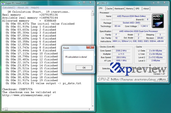
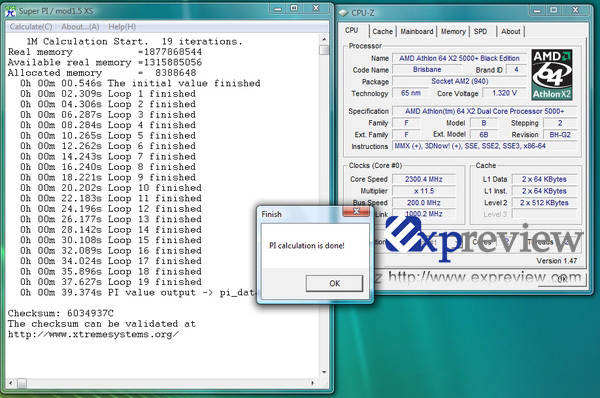
TSMC Expanding 28 nm Manufacturing Facility

With the advent of highly-complex 28 nm discrete PC graphics processors, and ARM designers lined up with their increasingly powerful SoCs, TSMC is bound to see a pile up of orders for chips built on its newest bulk manufacturing process. In view of this, the "messiah of the fabless" is planning an expansion of its 28 nm manufacturing facility. This expansion is set to occur a little later in 2012. TSMC reportedly is running at full capacity at its 12-inch fabs because of strong demand for 28 nm as well as 40 nm and 65 nm. Due to this, some designers are approaching TSMC's competitors UMC and Samsung for 28 nm bulk manufacturing, according to sources. The expansion will follow a revision of TSMC's capex target for 2012, up from US $6 billion.

Micron Debuts World's Highest-Density, High-Performance SPI NOR Flash Memory at 1 Gb

Micron Technology, Inc., today introduced the highest-density Serial Peripheral Interface (SPI) NOR memory available, launching 1 gigabit (Gb), 512 megabit (Mb) and 256Mb products in both 1.8V and 3V power supply voltages. Employing state-of-the-art 65nm process technology, the N25Q product family offers the highest-speed quad I/O in the industry and a full set of advanced features and small packages that improve overall system performance and time-to-market in networking, set-top boxes, automotive and a wide range of industrial, computing and consumer applications.

Extending the company's legacy of memory leadership, Micron's new SPI NOR product line balances customers' needs for cost-effective solutions at higher densities while ensuring compatibility among future chipsets. Micron's long-term commitment to customers in the embedded markets is reinforced by Micron's Product Longevity Program (PLP) - a 10-year commitment to provide stable memory architectures for customer designs. The new N25Q products will be offered as part of this program to provide design assurance for its PLP customers.

Spansion Announces Industry's First 4 Gb NOR Flash Memory

Spansion Inc., today announced the industry's first single-die 4Gb (gigabit) NOR Flash memory product at 65nm. The 4Gb Spansion GL-S delivers high-quality and fast read performance to enable a better user experience with interactive graphics, animation and video in games and automotive applications.

The newest addition to the flagship Spansion GL-S product line is sampling this month. Based on Spansion's proprietary, highly reliable MirrorBit charge-trapping technology, the Spansion GL-S delivers the fastest read performance in the industry, up to 45 % faster read than competing NOR Flash products. The Spansion GL-S family is currently offered at 128Mb through 2Gb densities and the company is gaining design win momentum for the product family with consumer, automotive, gaming, telecom and industrial applications.

Samsung Unveils New Wireless USB Chipset, Provides Higher Speeds, at Lower Power Draw

Samsung Electronics Co., Ltd., a worldwide leader in advanced semiconductor technology solutions, today introduced its latest wireless universal serial bus (USB) solution, developed using Ultra Wide Band (UWB) technology. Offered in a two-chip set, Samsung's newest S3C2680/ S5M8311 WUSB solution enables high definition content to be wirelessly transmitted from a mobile host device to a tethered device for viewing. Initial applications are high-resolution cameras, camcorders, TVs and PCs with prospects for adoption in other applications including tablet PCs, printers, beam projectors, portable HDDs, Blu-ray players, and mobile handsets.

"The ability to handle wireless high-speed data transmission while consuming less power is a key requirement for many consumer electronic devices," said Yiwan Wong, vice president, System LSI marketing, Samsung Electronics. "Due to power/performance issues, previous generations of WUSB products were unable to meet the consumers' expectations. Samsung's new WUSB chipset delivers up to 480Mbps (Megabit per second) data transmission rate, at an average power consumption of less than 300mW. This level of power efficiency greatly increases the attractiveness of WUSB connectivity in consumer electronic and mobile applications.

LSI and Seagate Co-develop Technology for Next-Generation High-Capacity HDDs

LSI Corporation and Seagate announced the delivery of a complex integrated read channel technology for Seagate's latest hard disk drive (HDD) products. Together, the companies have enabled the industry's first hard disk drives with low-density parity check (LDPC) read channel in 65nm process system-on-chip (SoC) technology.

The co-development effort combines Seagate LDPC digital back-end read channel and hard drive controller IP with LSITM analog front-end read channel (RC) and physical layer (PHY) technology. The combined LDPC read channel has been incorporated into high-capacity SoC solutions that enable new levels of performance and storage capacity for leading-edge Seagate HDDs.

Elpida Completes Development of 65nm XS Version 1-Gb DDR3 SDRAM

Elpida Memory, Inc., Japan's leading global supplier of Dynamic Random Access Memory (DRAM), today announced that it had completed development of a 65nm XS extra-shrink version 1-Gigabit DDR3 SDRAM that is as cost-competitive as 50nm process memory devices.

In response to the slump in the DRAM market that has lasted since 2008, Elpida is taking a two-track R&D approach that focuses on conventional process migration and on layout innovations that reduce the cost of capital investment. Along with migrating to advanced processes such as 50nm and 40nm the company is developing shrunken chip versions through extensive use of existing ArF dry scanner equipment. As a result, a 65nm S shrink version was developed in 2008 and now a 65nm XS extra-shrink version has been completed.

The 65nm XS is a smaller version of the already shrunken 65nm S and delivers 25% more chips per 300mm wafer compared with its predecessor. In addition to its extremely small chip size the XS shortens the manufacturing process and helps to greatly reduce equipment costs through the use of ArF dry scanner equipment. Chips costs are comparable to 50nm process products.

VIA Preparing Dual-Core Nano 3000 Processor for H2 2009

VIA, the third active player in the x86 processor market, is known for its low-power processors catering to the ULPC segment of the market. Sources tell HKEPC that the firm is now readying a dual-core variant of its Intel Atom competitor, the Nano 3000. The Nano 3000 series, slated for launches throughout 2009 includes a new architecture by VIA, while bearing the same essential Nano-BGA package.

The processor would use a boarder system interface with the 1333 MHz VIA V4 bus (FSB). It will feature x86-64 extension along with the SSE4 instruction sets to make it standards compliant. It will feature 128KB of L1 and 1MB of L2 caches. VIA is also looking to improve the processor's number-crunching capabilities by working on its integer and floating-point operations efficiency. The processor will be built on the Japanese Fujitsu 65nm manufacturing process which has so far been VIA's foundry partner with processors and S3 Graphics products. The company is also considering a switch to the TSMC 40nm or 45nm node later, sources note. The VIA Nano 3000 Dual-Core variant can be expected in the second-half of 2009, while single core variants of the architecture can be expected earlier.

G92-Based GeForce 9 Series Products to be Renamed GeForce GTS 200 Series

The NVIDIA G92 graphics processor has had the reputation of spanning across two generations of GeForce graphics accelerators, which could well become three with talk about NVIDIA executing another re-branding to products based on the GPU. The re-branding will use the B1 revision of the G92 GPU (aka G92b), which is known to have been manufactured on the 55nm fabrication process, along with the 65nm A1 revision.

The new series created will include two SKUs based on the G92, the GeForce GTS 240 and GeForce GTS 250. These are the 112 SP and 128 SP variants of the G92 core, presently branded under 8800/9800 GT and 8800 GTS 512, 9800 GTX/GTX+ respectively. NVIDIA looks to capitalise on the sales improvement the GTX 200 series has seen for the past two or so months now, by giving it a present-generation branding. The re-branding, or rather, releasing products with the new naming scheme is said to be operationalised by February 2009.

First Dual-Core Celeron Mobile CPUs Out

Intel has introduced its first set of mobile dual-core CPUs under the Celeron M branding. There are two models up for sale: T1700 and T1600, clocked at 1.83 GHz and 1.66 GHz respectively. These processors, based on the Core micro-architecture, have a shared L2 cache of 1 MB. These chips have a front-side bus speed of 667 MHz. Both these processors are derived from the 65nm silicon fabrication process, and come with rated TDP of 35W. The T1700 and T1600 are priced at US $86 and $80 respectively (in 1000 unit tray quantities), and are intended to be value offerings towards a segment of notebooks.

Intel to Phase Out Two More 65nm CPUs - the Core 2 Quad Q6700 and Core 2 Duo E4700

After outlining the phase out schedule for its Core 2 Quad Q6600 processor, Intel today reported that it is retiring two more CPUs - the 2.66GHz Core 2 Quad Q6700 Kentsfield (65nm) quad-core and the 2.6GHz Core 2 Duo E4700 Allendale (65nm) dual-core. Intel will be taking orders for both processors until March 24, 2009 and shipping them until June 4, 2010 in trays, and until July 3, 2009 boxed.

Xbox 360 Jasper Revision Hits Retail

The long rumored Jasper version of Microsoft's Xbox 360 gaming console has finally hit retail shelves. Up until now, we knew almost everything about Jasper, but non of us knew how to recognize the console, or if it was retailing at all. No official information was released, but xbox-scene report claims that Jasper Xbox 360s are finally arriving in stores. The revised console comes bundled with a new 150W (12.1A whereas old model draw 14.2A) power supply that is 25W less powerful than the power supply bundled with previous generation Falcon consoles. The new power supply is almost 100% proof that the console you're looking is Jasper. Also, according to the report all consoles manufactured after October 23rd 2008 with LOT number 0843X and manufactured from FDOU, should be a Jasper. At last, let us remind what Jasper means. That's the official code name for the last generation Xbox 360 consoles. Falcon consoles come with new 65nm GPU (90nm in previous generation) that produces less heat. Jasper consoles also should utilize new revised cooler and internals that will reduce the overall temperature and noise coming from it. Finally, with Jasper, we don't have to worry for the RRoD (Red Ring of Death) failure anymore.

Intel to Phase Out its Core 2 Quad Q6600 Processor Next Year

DigiTimes reports that Intel is to phase out its most beloved 65nm 2.4GHz Core 2 Quad Q6600 processor in the first quarter of 2009.
Intel is planning to start phasing out the 65nm Core 2 Quad Q6600 in the first quarter of 2009, prompting several PC and channel vendors to start planning to cut Q6600-product prices to clear their inventory before the end of this year, according to sources at PC vendors.
Intel will issue a product discontinuance notice for the Q6600 in the first quarter next year, and call end-of-lifecycle in the second quarter.
Acer has reduced pricing for its Intel Core 2 Quad Q6600-based desktops to below NT$13,900 (US$418) for the IT Month consumer show in the Taiwan market, and other vendors are expected to follow suit.

Intel Discontinues Several 45nm and 65nm Core 2 Duo Processors

Intel recently issued a list of the processors it will be phasing out in favour of the new and faster Core i7 CPUs. The list includes several 65nm, 45nm and some laptop processors:
  • Q9450 (2.66 GHz 1333 MT/s, quad-core, 95 watt, LGA775, Yorkfield 45nm)
  • E8200 (2.66 GHz 1333 MT/s, dual-core, 65 watt, LGA775, Wolfdale 45nm)
  • E8190 (2.66 GHz 1333 MT/s, dual-core, 65 watt, LGA775, Wolfdale 45nm)
  • E6850 (3.00 GHz 1333 MT/s, dual-core, 65 watt, LGA775, Conroe 65nm)
  • E6750 (2.66 GHz 1333 MT/s, dual-core, 65 watt, LGA775, Conroe 65nm)
  • E6550 (2.33 GHz 1333 MT/s, dual-core, 65 watt, LGA775, Conroe 65nm)
  • E6540 (2.33 GHz 1333 MT/s, dual-core, 65 watt, LGA775, Conroe 65nm)
  • E4600 (2.40 GHz 800 MT/s, dual-core, 65 watt, LGA775, Allendale 65nm)
  • T7400 (2.16 GHz 667 MT/s, mobile dual-core, 34 watt, Socket-M, Merom 65nm)
  • Celeron-M 530 (1.73 GHz mobile, 533 MT/s, single-core, 30 watt, Socket-M, Merom-1024 65nm)
You will still be able to get these items until 2010, but Intel is already taking measures to slowly phase them out from the market.

More Details on AMD's 45nm CPU Line-up Revealed

Industry informer DigiTimes shared today some information on the upcoming Deneb processor family from AMD. According to their information, AMD is planning to launch six high-end 45nm quad-core CPUs (Deneb) and four entry-level (Propus) including 20x00, 18x00, 16x00 and 1xx00e models, in the first quarter of next year. Two of these processors will be available earlier in November of this year - the 3GHz Phenom X4 20550 and 2.8GHz 20350 for socket AM2+ systems.
AMD will also launch six 45nm triple-core CPUs (Heka and Regor) including 14x00, 12x00 and 1xx00e series. These triple-core CPUs will enter design validation test (DVT) and start shipping in the first quarter next year.
In the second and third quarter of next year AMD will also start shipping its 45nm AM3-based dual-core CPUs, part of the Regor family.
Although the chipmaker will largely enter the 45nm generation, in order to prevent potential yield rate problems from the new process, it will launch seven 65nm CPUs including three quad-core Phenom X4 CPUs (Agena) - 9950 (120W), 9850 (95W) and 9450e (65W), and two Athlon X2 CPUs (Kuma) - 7750 and 7550 in the first quarter of 2009, while two low-power Athlon X2 CPUs (Brisbane) - 5050e and 3250e, will launch in the near future.
Launching of the new Phenom processors will also lead to new price reductions and last order notices for some of the older processors. Unfortunately, there is no additional information.

Intel Prepares to Phase Out Thirty One 65nm Server Xeon Processors

Intel informed today that it will be phasing out a large number of server Xeon processors during the next eight months. That's mainly because of the forthcoing Nehalem platform and the new Core i7 processors. Intel also said that it is already producing more 45nm processors than 65nm chips, so it's time for some of the 65nm parts to drop off the charts. The list includes six dual-core Xeon processors with Woodcrest core, these are the 1.86GHz Xeon 5120, 2.66GHz 5150, 2.33GHz LV 5148, 1.60GHz 5110, 2.0GHz 5130, 2.33GHz 5140 and 3.0GHz 5160. The list continues with nine quad-core models with Clovertown core, the 1.86GHz E5320, 1.86GHz L5320, 3.0GHz X5365, 2.66GHz X5355, 1.60GHz E5310, 2.33GHz E5345, 2.0GHz E5335 and 2.0GHz L5335. Sales of different variations of these CPUs are also going to be phased out. The total count is 31 server models, that won't be produced anymore. Final customer orders for these processors can be submitted until April 23, 2009. Intel plans the final shipment of these processors for July 23, 2009.

Elpida Completes Development of 65nm Chip Shrink

Elpida Memory, Japan's leading global supplier of Dynamic Random Access Memory (DRAM), announced today that it has developed a shrunken version of its 1-gigabit DDR2 SDRAM that delivers 20% more chips from a single 300mm wafer. Volume production of the new shrunken chip is expected to begin before the end of 2008 and will be shared among Elpida's Hiroshima Plant, its Taiwan-based Rexchip joint venture and its manufacturing partner PSC.

Phenom X4, X3 45nm Lineup for H1 2009 Explained

AMD would be releasing its first desktop processors based on the 45nm silicon fabrication process, based on the newer Deneb core. The company is said to have made several tweaks to the original K10 design and equipped the core with 300% the amount of L3 cache as its 65nm Agena parts. The only thing got us wondering was what would be its nomenclature like? Well, be surprised to know that after Phenom X4 9000 series, the company plans to continue the numbering with a 5-digit model number scheme with x1000 unit deviations between models. A rather confusing naming scheme, as suggested by the chart provided, seems to have been adopted.

It is now clear, that there will be two distinct kinds of Phenom X4 45nm chips: those which continue support for DDR2 memory on the existing AM2/AM2+ sockets, and those which are exclusive to the AM3 socket and feature support for DDR3 memory, DDR3 1333MHz at that. The processors would feature dual 64-bit memory controllers, which could be ganged for a single 128-bit wide memory interface, or un-ganged to step up multi-tasking efficiency.

Phenom X2 Churns out Roughly 15% Increments with Super Pi

Phenom X2 is intended to be the latest dual-core processor from AMD. It is based on the newer K10 architecture. The 65nm Kuma core is what sits inside the first to release models of the Phenom X2. Although based on K10 architecture and Kuma core, the initial batch being 65nm, AMD for some reason chooses to call it Athlon X2 saving the Phenom brand name perhaps for the 45nm batches? At least the sample Expreview got had the Athlon X2 etching on it. The chip carried the "AD6500" label and came with a 2.30 GHz clock speed.

Here's something to ponder: 6500 isn't a performance rating, it is just a model number. The Athlon 64 X2 6400+ had a 3.20 GHz clock speed. As performance evaluations will soon show, the Phenom/Athlon 6500 isn't anywhere close to the performance of the X2 6400+. However, architectural improvements meant that Kuma outperforms Brisbane (K8, 65nm) on a clock to clock basis. To ascertain this, Expreview used a Athlon 64 X2 5000+ Black Edition (Brisbane) that was underclocked to 2.30 GHz, the clock speed which AD6500 comes with. Super Pi 1M benchmark was run. While the Brisbane chip crunched it in 39.374 s, Kuma did it in 33.43 s indicating a performance increment of roughly 15%. The test-bed consisted of a NVIDIA nForce 750a SLI motherboard and GEIL 1GB DDR2-800 memory. Kuma AD6500 comes with a shared L3 cache of 2 MB apart from dedicated L2 caches of 512 KB per core. It uses a broader HyperTransport 3.0 system interface at 3600 MT/s. It supports DDR2-1066.

AMD 45nm Deneb Consumes up to 12% Less Power Compared to 65nm Agena

The newest fleet of quad-core desktop processors from AMD, the Deneb series is tested by Chinese website Zol to consume up to 12 per cent less power compared to equally clocked 65nm Agena parts, add to that, the fact that the 45nm Deneb comes with three times the amount of L3 cache, 6 MB.

The 45nm and 65nm parts were compared on a MSI K9A2 Platinum motherboard with a NVIDIA GeForce GTX 280 card, a single 320 GB HDD, two modules of 1GB DDR2 1066 MHz memory, the test-bed was powered by a Thermaltake Toughpower 1200W PSU. Power consumption was calculated in idle and load (the CPUs were stressed using instances of Orthos).

Report: Microsoft Prepares to Release the 65nm Xbox 360 ''Jasper'' Consoles in August

The China Economic News Service reported today that Microsoft has assigned Taiwan Semiconductor Manufacturing (TSMC), Advanced Semiconductor Engineering (ASE) and Nanya PCB to manufacture, test and package the latest version of Xbox 360, codenamed "Jasper". TSMC will build ATI Xenos graphics and memory controller hub (GMCH) for the new Jasper console, using 65nm process. ASE was contracted to package and test the two chips, while Nanya has won orders to supply flip-chip packaging substrates, reports CENS.com. Current Xbox 360 consoles named Falcon utilize GMCH and eDRAM cores manufactured using 90nm process technology at TSMC as well as CPU built at IBM using 65nm fabrication process. The new Jasper Xbox 360s are projected to consume less electricity, use less complex cooling systems and logically produce less noise. In addition the revised consoles will fix the so-called "red ring of death" issue that plagued many Falcon systems. Microsoft will reportedly make available the Jasper version of XBox 360 game console in August this year.

Intel Drops 65nm Processor Prices

Intel slashed today the prices of its 65nm Core 2 Duo and Core 2 Quad Q6600/Q6700 Kentsfield processors. The tray price of the Q6600, which has been the universal quad-core in Intel's line-up for more than a year, was dropped 16% from $266 to $224. More important than the Q6600 drop, Q6700 which had a tray price of $530 now costs $266 - almost 50% cheaper.
Other price reductions include the 65nm, 3.0GHz Core 2 Duo E6850 (-31% to $183), which now matches the price of the 45nm E8400 (3.0GHz) as well as the Pentium E2200 (-12% to $74), the E2180 (-14% to $64), the Celeron 560 (-20% to $107), the Celeron 550 (-20% to $86), the Celeron 440 (-17% to $44) and the Celeron 430 (-23% to $34).

40GB PS3 Does Use 65nm Processors After All

None of the console manufacturers have really been very open in regards to their CPU micro architecture. However, when rumors went around that Sony was filling the 40GB PS3s with 90nm processors as if it was a bad thing, Sony was very prompt in dispelling such rumors. They announced in an interview that the Cell processor in the 40GB PS3 was indeed on 65nm technology, dropping power consumption by an impressive 100W. The NVIDIA RSX chip, though, still is on a 90nm processor, which is why people assumed the entire 40GB PS3 was still on a 90nm process.
Return to Keyword Browsing
Apr 18th, 2024 18:53 EDT change timezone

New Forum Posts

Popular Reviews

Controversial News Posts