News Posts matching #Cypress

Return to Keyword Browsing

Sound from Ultrasound: Audio Pioneer xMEMS' New Silicon Speaker Reinvents How Humans Experience Sound

xMEMS Labs, pioneers in solid-state, all-silicon micro speakers, today announced a revolutionary breakthrough in sound reproduction, changing the way mass-market, true wireless stereo (TWS) earbuds create ultra high-quality, high-resolution sound experiences across all audio frequencies.

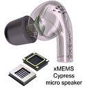
With the introduction of its groundbreaking new Cypress solid-state MEMS speaker, xMEMS engineers have replaced legacy push-air sound reproduction with the company's ultrasonic amplitude modulation transduction principle. Ultrasonic modulation turns ultrasonic air pulses into rich, detailed, bass-heavy, high-fidelity sound, representing the first no-compromise alternative to the moving-coil concept for high-volume consumer active noise canceling (ANC) earbud micro speakers.

XMG Reports Higher Availability of Ryzen 5000 Mobile Processors

Laptop manufacturer XMG Has recently reported that the supply of AMD Ryzen 5000 mobile processors has increased considerably in the past weeks with this availability expected to continue through the coming months. These supply improvements come after an ongoing period of global chip shortages which has resulted in price increases for various electronics devices. XMG also reports that the supply of components from Intel and NVIDIA is expected to remain stable but ICs from Realtek and Cypress continue to fluctuate in availability and pricing.
XMGThe availability of AMD's current mobile processors from the Ryzen 5000 series has improved significantly over the past few weeks. The coming months continue to promise a reliable CPU supply.

Intel Core i7-11700K "Rocket Lake" CPU Outperforms AMD Ryzen 9 5950X in Single-Core Tests

Intel's Rocket Lake-S platform is scheduled to arrive at the beginning of the following year, which is just a few days away. The Rocket Lake lineup of processors is going to be Intel's 11th generation of Core desktop CPUs and the platform is expected to make a debut with Intel's newest Cypress Cove core design. Thanks to the Geekbench 5 submission, we have the latest information about the performance of the upcoming Intel Core i7-11700K 8C/16T processor. Based on the Cypress Cove core, the CPU is allegedly bringing a double-digit IPC increase, according to Intel.

In the single-core result, the CPU has managed to score 1807 points, while the multi-core score is 10673 points. The CPU ran at the base clock of 3.6 GHz, while the boost frequency is fixed at 5.0 GHz. Compared to the previous, 10th generation, Intel Core i7-10700K which scores 1349 single-core score and 8973 points multi-core score, the Rocket Lake CPU has managed to put out 34% higher single-core and 19% higher multi-core score. When it comes to the comparison to AMD offerings, the highest-end Ryzen 9 5950X is about 7.5% slower in single-core result, and of course much faster in multi-core result thanks to double the number of cores.

Intel to Keep Its Number One Semiconductor Supplier Ranking in 2020: IC Insights

IC Insights' November Update to the 2020 McClean Report, released later this month, includes a discussion of the forecasted top-25 semiconductor suppliers in 2020. This research bulletin covers the expected top-15 2020 semiconductor suppliers (Figure 1).

The November Update also includes a detailed five-year forecast through 2024 of the IC market by product type (including dollar volume, unit shipments, and average selling price) and a forecast of the major semiconductor industry capital spenders for 2020. A five-year outlook for total semiconductor industry capital spending is also provided.

Intel Confirms Rocket Lake-S Features Cypress Cove with Double-Digit IPC Increase

Today, Intel has decided to surprise us and give an update to its upcoming CPU lineup for desktop. With the 11th generation, Core CPUs codenamed Rocket Lake-S, Intel is preparing to launch the new lineup in the first quarter of 2021. This means that we are just a few months away from this launch. When it comes to the architecture of these new processors, they are going to be based on a special Cypress Cove design. Gone are the days of Skylake-based designs that were present from the 6th to 10th generation processors. The Cypress Cove, as Intel calls it, is an Ice Lake adaptation. Contrary to the previous rumors, it is not an adaptation of Tiger Lake Willow Cove, but rather Ice Lake Sunny Cove.

The CPU instruction per cycle (IPC) is said to grow in double-digits, meaning that the desktop users are finally going to see an improvement that is not only frequency-based. While we do not know the numbers yet, we can expect them to be better than the current 10th gen parts. For the first time on the Intel platform for desktops, we will see the adoption of PCIe 4.0 chipset, which will allow for much faster SSD speeds and support the latest GPUs, specifically, there will be 20 PCIe 4.0 lanes coming from the CPU only. The CPU will be paired with 12th generation Xe graphics, like the one found in Tiger Lake CPUs. Other technologies such as Deep Learning Boost and VNNI, Quick Sync Video, and better overclocking tuning will be present as well. Interesting thing to note here is that the 10C/20T Core i9-10900K has a PL1 headroom of 125 W, and 250 W in PL2. However, the 8C/16T Rocket Lake-S CPU also features 125 W headroom in PL1, and 250 W in PL2. This indicates that the new Cypress Cove design runs hotter than the previous generation.

Intel Rocket Lake CPUs Will Bring up to 10% IPC Improvement and 5 GHz Clocks

Intel is struggling with its node development and it looks like next-generation consumer systems are going to be stuck on 14 nm for a bit more. Preparing for that, Intel will finally break free from Skylake-based architectures and launch something new. The replacement for the current Comet Lake generation is set to be called Rocket Lake and today we have obtained some more information about it. Thanks to popular hardware leaker rogame (_rogame), we know a few stuff about Rocket Lake. Starting off, it is known that Rocket Lake features the backport of 10 nm Willow Cove core, called Cypress Cove. That Cypress Cove is supposed to bring only 10% IPC improvements, according to the latest rumors.

With 10% IPC improvement the company will at least offer some more competitive product than it currently does, however, that should be much slower than 10 nm Tiger Lake processors which feature the original Willow Cove design. It shows that backporting of the design doesn't just bring loses of the node benefits like smaller design and less heat, but rather means that only a fraction of the performance can be extracted. Another point that rogame made is that Rocket Lake will run up to 5 GHz in boost, and it will run hot, which is expected.

Cypress Ships its One Billionth USB-C Device

Cypress, an Infineon Technologies Company, today announced that in less than five years, the company has achieved a landmark milestone by shipping its one billionth USB-C device. As the leading provider of USB-C technology, Cypress' leadership position spans a wide range of markets with its controllers used within mobile, computing, and power applications.

Cypress offers the industry's most complete portfolio of USB solutions, including device controllers, embedded hosts, hubs, application-specific bridges, and transceivers. Cypress' EZ-PD portfolio was the first in the industry to support the latest USB Power Delivery (USB PD) 3.0 specification, which enables more robust end-to-end power delivery and charging solutions for laptop and mobile devices. Cypress also offers AEC-Q100 certified versions of its controllers for automotive-grade performance.

'Spectra' Cyber Attack Breaks Coexistence Between Wi-Fi and Bluetooth

Nowadays wireless technologies are increasingly sharing spectrum. This is the case for Wi-Fi and Bluetooth, but also some LTE bands and harmonics. Operating on the same frequency means that these different technologies need to coordinate wireless spectrum access to avoid collisions. Especially for nearby sources, as it is the case for multiple chips within one smartphone, so-called coexistence is the key to high-performance spectrum sharing.

Coexistence between wireless chips can be implemented in various ways. While there are open specifications, most manufacturers opt to develop proprietary coexistence mechanisms to further improve performance. Open interfaces are not needed on combo chips that implement multiple wireless technologies, as the manufacturer has full control.

Spectra, a new vulnerability class, relies on the fact that transmissions happen in the same spectrum and wireless chips need to arbitrate the channel access. While coexistence should only increase performance, it also poses a powerful side channel.

Cypress and EverPro Extend USB 3.0 Performance Up to 100 Meters

EverPro Technologies Ltd., a leader in USB 3.0 transmission solutions, and Cypress Semiconductor Corp., today announced the completion of successful interoperability testing between both Cypress's EZ-USB FX3 USB 3.0 peripheral controller and EZ-USB CX3 camera controller and EverPro's U3C A0A0-100 USB 3.0 active optical cable (AOC). EverPro is demonstrating the U3C A0A0-100 solution at the 9th China International Machine Vision Exhibition here in Shenzhen from June 18 to June 20, 2014.

USB 3.0 is gaining popularity in machine vision and industrial cameras thanks to its 5 Gbps bandwidth that enables high-resolution, high-frame-rate imaging in real time without the need for compression, which degrades image quality. However, USB 3.0 currently has a maximum cable length of 3 meters that has limited its adoption. EverPro's USB 3.0 transmission solution with active optical cable technology overcomes this limitation and extends full USB 3.0 performance up to 100 meters. This cable length extension allows Cypress USB 3.0 solutions to be easily and cost effectively deployed across a wider range of machine vision and industrial applications, removing cable length limitations in camera placement and installation.

Cayman Confirmed To Be Using VLIW4 SP Arrangement, Redesigned ROPs

With the introduction of AMD's Radeon HD 6000 series GPUs, we were made to expect a massive architectural change in the way AMD arranges its unified shaders. That, however, didn't happen with the Radeon HD 6800 series based on the 40 nm "Barts" GPU, which continued to maintain the VLIW5 configuration (comprising of SIMD units with 4 simple and 1 complex stream processing units). A recent presentation leaked to the internet reveals that the much talked about architectural change was saved for Cayman, the company's upcoming high-end GPU, on which will be based Radeon HD 6900 series graphics cards.

In VLIW4 architecture, equipotent stream processing units are arranged in groups of four along with general purpose registers. Although the four have equal capabilities, two out of four of these (occupying 3 and 4 issue slots) are assigned with some special functions. AMD looks to be conservative with the benefits of the new SIMD architecture. It claims that VLIW4 gives similar computational power as VLIW5, with 10% reduction in die area. It also simplifies scheduling.

Radeon HD 6870 PCB and GPU Pictured

The fine folks at IT168 revealed the first pictures of the Radeon HD 6870 PCB with its cooler completely off, and in its production livery (black). Also let out is the first [clear] picture of the GPU itself. The PCB was first pictured in its nascent qualification sample form, with a development GPU cooler on. The final version of the PCB sticks to its qualification sample for the most part, it has VRM components positioned forwards, trailed by the GPU and its memory. The card makes use of a 4+1+1 phase VRM. All eight memory chips are on the obverse side, each with its own 32-bit wide path, since there's a 256-bit memory interface.

The GPU package is of the same dimensions as the Cypress package, albeit a smaller die. We're getting to hear that Barts is pin-compatible with Cypress (meaning that a Barts GPU can be placed onto a Cypress PCB, given the appropriate BIOS, and it will work), however, no AIB is likely to reuse Cypress PCBs other than for Eyefinity6 designs, because while Barts can make do with a 6-layer PCB, close to every existing Cypress PCB is an 8-layer one, and that Cypress PCBs lack the second mini-DP connector. The die is placed diagonally on the package (à la Cypress and R600), it is rectangular, while the Cypress die is more or less square. ChipHell.com contributor musicinlove did a nice size measurement and comparison. Finally, the AMD "arrow" logo is etched onto the die, it's curtains down for ATI.

ATI Radeon HD 6000 Series GPU Codenames Surface

Even as NVIDIA is taking its own sweet time to complete building its lineup of DirectX 11 compliant GPUs to target all market segments, AMD, which got a 6 months' headstart into releasing its lineup, which ended up targeting all market segments in a span of 5 months, is readying the Radeon HD 6000 series for launch well within this year. Just as the Radeon HD 5000 series GPU family was codenamed Evergreen with its members codenamed after evergreen trees (such as Cypress, Juniper, Redwood, Cedar), the Radeon HD 6000 is codenamed "Southern Islands", with its members codenamed after islands in the Caribbean (not islands in the Mediterranean).

"Bart" (after Saint Barthélemy island) is the codename for the performance/upper-mid segment GPU, a successor to the "Juniper" Radeon HD 5700 series. "Cayman" (after Cayman Islands) is the enthusiast GPU, successor to Cypress, and will go into making SKUs that succeed the Radeon HD 5800 series. Finally, the king of the hill is codenamed "Antilles" (after Antilles Islands), it is the dual-GPU SKU that makes use of two Cayman GPUs, successor to the Radeon HD 5970 "Hemlock". AMD partners will be in a position to sell graphics cards based on these by November 2010. The Radeon HD 6970 "Antilles" should be out by December 2010. The lower-half of the family will likely release next year.

ASUS ROG Matrix HD 5870 Further Detailed

ASUS has been readying its Republic of Gamers (ROG) Matrix HD 5870 graphics card. Earlier, the card was pictured fully assembled. Sources shared pictures of the card taken apart, showing its PCB and cooling assembly from the inside, which tells us a lot about this card. To begin with, ASUS engineered this card from scratch, with its own PCB and cooler designs, and choice of components. The card comes overclocked out of the box, and also promises overclocking headroom higher than the reference design. It features 2 GB of GDDR5 memory. The PCB reveals a strengthened VRM. There is a 10-phase vGPU and 2-phase vMem, with independent voltage controllers. Power is drawn in from two 8-pin power inputs.

Sapphire Readies Custom HD 5970 with 4 GB memory, HD 5870 Eyefinity6, for CeBIT

Sapphire is readying a bundle of interesting new graphics products to be unveiled at this year's CeBIT event. Two such products that stand out include a non-reference design Radeon HD 5970 accelerator with 4 GB of GDDR5 memory (2 GB per GPU), and the HD 5870 Eyefinity6 2 GB. The HD 5970 model is particularly interesting, as its rival in the field, ASUS, will be showing off a similar accelerator called the ROG Ares "dual HD 5870" accelerator. Sapphire however, prefers to call its creation a custom Radeon HD 5970. It is expected to feature custom cooling, increased clock speeds (and probably overclocking headroom), and twice the amount of memory. There is a likelihood that Sapphire designs this along the lines of its high-end "Atomic" series that includes watercooling, and other exclusive features.

The other offering by Sapphire of course is the HD 5870 Eyefinity6. Probably sticking to AMD's reference design, the Eyefinity6 card is optimised for ATI Eyefinity setups with up to six physical displays. The card has six mini DisplayPort connectors, with which it can connect to each of its display heads. It features 2 GB of GDDR5 memory across a 256-bit wide interface. Using AMD Cypress GPU, it packs 1600 stream processors, 80 TMUs, and 32 ROPs. At the same event, Sapphire will show off several other of its new creations, such as the N450 netbook, Mini Projector 101, and mini-ITX form-factor motherboards supporting socket AM3.

AMD Gives out WHQL Driver for Radeon HD 5830

Outside its monthly driver release cycle, AMD released a WHQL-signed driver based on ATI Catalyst 10.2, which adds support for the Radeon HD 5830 graphics processor. It retains the feature-set and bug-fixes packed in Catalyst 10.2, with support for the new GPU being just appended to it. The driver supports Windows XP, Vista, 7, and Linux.

Released yesterday, the ATI Radeon HD 5830 is the cost-effective member of the Radeon HD 5800 series. It is based on the Cypress LE GPU, with 1120 stream processors, 56 TMUs, 16 ROPs, 256-bit GDDR5 memory interface to connect to 1 GB of memory, apart from the entire feature-set of the Radeon HD 5800 series.

DOWNLOAD: ATI Radeon HD 5830 driver based on Catalyst 10.2 WHQL for Windows 7/Vista | Windows XP

ASUS Designing Dual-HD 5870 Graphics Accelerator?

ASUS is known to toy with bleeding-edge technology to give out high-end products. Earlier, ASUS put two GeForce GTX 285 GPUs into one accelerator to give out a custom-design product that outperformed NVIDIA's dual-GPU GeForce GTX 295. According to o.v.e.r.clockers.at, ASUS might be doing something similar, this time around with AMD's Cypress GPUs in its Radeon HD 5870 avatar. It is said to be working on a dual-HD 5870 graphics card, codenamed "Ares".

While the dual-GPU Radeon HD 5970 uses full-featured AMD Cypress GPUs (with all its stream processors and memory bus width available), ASUS will attempt to use the one disparity between an HD 5970 and two HD 5870 to its advantage: clock speeds. The Cypress GPUs in HD 5970 feature lower clock speeds (725/1000 MHz core/memory) compared to the single Cypress GPU on the HD 5870 (850/1200 MHz). Electrical constraints are probably the reason behind this. It is likely that ASUS will use stronger VRM circuitry to power the two GPUs to run at higher speeds, while also providing some overclocking headroom.

AMD in a recent conference call to the press said that it didn't expect to see custom-design HD 5970-like accelerators till Q2 2010, although we don't infer there to be any sort of restriction in place, as was the case with NVIDIA and its GTX 295. Ares is likely named after the Greek God of warfare by the name. An apt successor to Mars (which also happens to be the name of the Roman God of war), ASUS' previous attempt at an extreme high-end graphics card of its own design.

Radeon HD 5700 Series Specs Surface

The beans are spilled on the final specifications of AMD's "Juniper" mid-range GPU architecture, and the two SKUs based on it, namely the ATI Radeon HD 5770 and Radeon HD 5750. Leaked alleged company slides on XtremeSystems Forums, reveal exactly how Juniper is a 50% downsizing of Cypress' machinery, in having half of nearly all its vital-statistics, if you may. Juniper features 10 SIMD engines physically, amounting to 800 stream processors. It holds 40 texture memory units (TMUs), and 16 raster operation units (ROPs). With a 128-bit memory interface churning out up to 76.8 GB/s of memory bandwidth by utilizing 4.8 GT/s GDDR5 memory chips, the fact that Juniper is half of what Cypress stands for specs-wise, becomes clear.

In the next two slides are pictured and detailed the two SKUs based on the GPU. The ATI Radeon HD 5770 is the top-end implementation, which makes use of all the components present on the GPU. With a core clock-speed of 850 MHz, and memory speed of 1200 MHz, the GPU churns out a shader compute power of 1.36 TFLOPs. The idle and max board powers are rated by AMD at 18W and 108W, respectively. It becomes clear that AMD is eying the US $150 price point with this part. The Radeon HD 5750 on the other hand, has one SIMD engine disabled, and eds up with 720 available stream processors. It comes with 1 GB or 512 MB of GDDR5 memory, and clock speeds of 700 MHz core, and 1150 MHz memory (4.6 GT/s). With these, the Radeon HD 5750 manages a shader compute power figure of 1.008 TFLOPs. The rated board power consumption figures have also come down on this one, with 16W idle, and 86W max. This one targets the $109 (512 MB) and $129 (1 GB) price points. Both accelerators are DirectX 11 compliant, and support ATI Eyefinity technology supporting up to three 2560 x 1600 pixel display heads. According to the slides, they should be unveiled this Tuesday the 13th.

ASUS HD 5870 Overclocks to 1035/1290 MHz on Air, Aces 3DMark Vantage in CrossFireX

Here is what four AMD Cypress GPUs can achieve with some careful overclocking, without needing any third-party cooling. Renowned overclocker Kinc sent us details of his latest achievement using four ASUS Radeon HD 5870 1 GB cards installed in a 4-way CrossFireX setup, all overclocked, and cooled by AMD's reference cooler, taking a shot at 3DMark Vantage (Extreme Preset). The four cards returned a score of X26,332 points, with an average frame-rate of 79.49 fps in GT1, and 74.83 fps in GT2.

To begin with the cards were overclocked to 1035/1290 MHz, up from reference speeds of 850/1200 MHz (core/memory). This was supported by raising the vGPU to 1.330V using GPUTool, from 1.015V. The platform to drive this feat comprised of an Intel Core i7 965 XE processor, cooled by Intel's reference (boxed) cooler, clocked at 4257 MHz. To seat them all was an ASUS P6T7 WS SuperComputer motherboard. The feat serves as a prelude to what the future holds in two "Hemlock" accelerators, which make use of two Radeon HD 5870 GPUs each.

AMD Radeon HD 5870 X2 Pictured

Behold AMD's, and soon aimed to be the industry's most powerful graphics accelerator: Radeon HD 5870 X2 "Hemlock". Armed with two "Cypress" Radeon HD 5870 graphics processors, this dual-GPU monstrosity packs twice the shader compute power. From the looks of it, the card is slightly longer than its single-GPU sibling from the series, and is better ventilated, although the cooler design more or less resembles it. It draws its power from one 6+2 pin and one 6 pin PCI-E power connectors, just like two of its ancestors in the R700 and R680. Listed for pre-order on a European online store, a Radeon HD 5870 X2 by Club3D is priced at 677 EUR (incl. applicable taxes, 568.9 EUR excluding).

AMD Cypress Graphics Accelerator Pictured

Here's the first sighting of a fully-assembled upcoming AMD Cypress "Radeon HD 5870" accelerator. This photo-shoot comes a couple of days ahead of its unveiling to the press tomorrow. Here's our very first thoughts on what we see:
  • The accelerator is unusually long for a single-GPU one from AMD. The company wouldn't splurge too much on aesthetics (especially lengthening the PCB), if there's no need for it to do so. Apparently there is.
  • Connectivity options galore. With two DVI-D, and one each of DisplayPort and HDMI, AMD promises it can handle three display-heads per GPU.
  • The components behind the GPU area (exposed) indicates the GPU to be somewhat large
  • History tells us that AMD uses a backplate only if it finds a real utility in it, such as cooling additional memory chips or VRM components. This card has a large, almost full-coverage backplate.
What surfaced months ago on sources such as ChipHell, which was then ridiculed for accuracy, has finally taken shape. If anything, Cypress does look like it means business. Expect further details to be out soon. Cypress is codename for AMD's next-generation DirectX 11 compliant graphics processor in the high-performance segment.

* Images removed at request of AMD *
Return to Keyword Browsing
Apr 26th, 2024 11:16 EDT change timezone

New Forum Posts

Popular Reviews

Controversial News Posts