News Posts matching #GK104

Return to Keyword Browsing

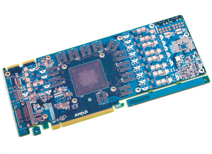
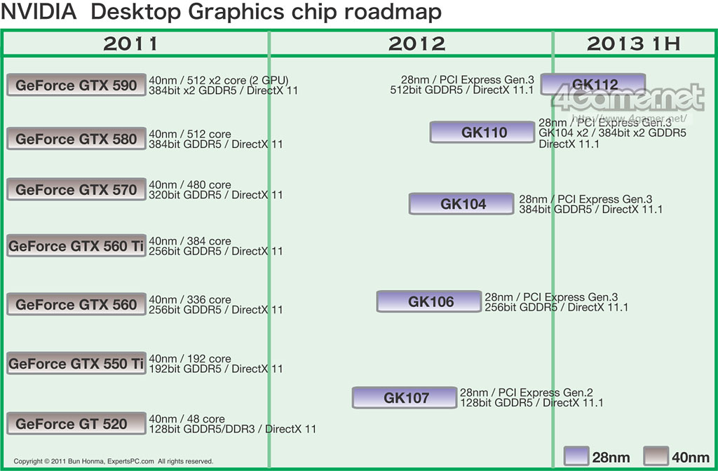
GK104-Based Products Arriving March 23

Expreview cited sources in the AIC (add-in card) vendors in pinning the launch of GeForce Kepler 104 (GK104) based products to March 23. The products launched are expected to be NVIDIA's first in its next-generation. Some label the top part based on GK104 as "GeForce GTX 670 Ti", while others call it "GeForce GTX 680". A March 23 launch explains reports of hectic activity in the green camp starting this week. NVIDIA typically enters NDAs with its partners over a wide time range, probably this one extends to April (since the launch is now reported to be towards late-March), which led some to believe Kepler was "delayed" to April. NVIDIA recently posted on its Facebook wall that people will be rewarded for their patience with an "unbeatable" product.

GK104 Board Draws Power From 6+8 Pin Connectors, 3+2 VDD Phase Power Supply

The top desktop graphics card based on the NVIDIA GeForce Kepler 104 (GK104) ASIC, which has come to be known as GeForce GTX 670 Ti, is reported to use a 5 NVVDD phase power supply (VRM) design that draws power from 6-pin and 8-pin power connectors. The card will hence have 300W of power at its disposal. NVVDD phase 1 and 3 will be wired to the 6-pin connector; phase 2, 4, and 5 to the 8-pin connector. NVVDD phases 2, 4, and 5 feed power to the GPU, while phases 1 and 3 power the GDDR5 memory and other components on the board.

Top NVIDIA GK104 Part Gets GeForce GTX 670 Ti Branding

NVIDIA has reportedly named the top desktop graphics card based on its upcoming 28 nm GK104 GPU GeForce GTX 670 Ti. The GK104 is a spiritual-successor to GF114 (which in-turn, to GF104), and NVIDIA is eager to get this part out fast, so it could consolidate on the performance thru high-end segment, before it's certain that it won't face issues with its foundry partners, so it could go ahead and launch parts based on the GK110. Interestingly, NVIDIA chose to name the highest-performing GK104-based SKU GTX 670 Ti and not GTX 660 Ti, probably indicating that this part will perform competitively with high-end parts out in the market today, including AMD's recently-launched Radeon HD 7000 series.

Speaking of performance, sources told SweClockers that they expect the GeForce GTX 670 Ti to outperform GeForce GTX 580 and Radeon HD 7950. Its specifications doing rounds on the web suggest it has a radically different number-crunching machinery. Industry analyst DigiTimes recently pinned launches of GeForce Kepler family to begin in April, though we're hearing there will be substantial activity surrounding these GPUs in March.

Radeon HD 7800 Series Inbound for March, NVIDIA Kepler in April: Report

AMD's Radeon HD 7800 series performance GPUs that target cost-benefit sweet-spots will be launched in the first half of March. The launch will include Radeon HD 7870 and Radeon HD 7850. The two SKUs are based on a new 28 nm ASIC codenamed "Pitcairn". Little is known about its specifications at this point, from reliable sources at least.

In April, AMD's rival NVIDIA will get its GeForce Kepler family of GPUs, all guns blazing. In April alone, NVIDIA is expected to launch a high-end part, the GeForce GTX 690, a performance part, the GeForce GTX 660, and mainstream part GeForce GTX 640. The three will be based on three new ASICs built on the 28 nm process, the GK110, GK104, and GK106, respectively.

April will be the most interesting month for PC enthusiasts as Intel will launch its third-generation Core processor family, codename "Ivy Bridge". Little is known about AMD's high-end Radeon HD 7990 "New Zealand".

NVIDIA GeForce Kepler Packs Radically Different Number Crunching Machinery

NVIDIA is bound to kickstart its competitive graphics processor lineup to AMD's Southern Islands Radeon HD 7000 series with GeForce Kepler 104 (GK104). We are learning through reliable sources that NVIDIA will implement a radically different design (by NVIDIA's standards anyway) for its CUDA core machinery, while retaining the basic hierarchy of components in its GPU similar to Fermi. The new design would ensure greater parallelism. The latest version of GK104's specifications looks like this:

SIMD Hierarchy
  • 4 Graphics Processing Clusters (GPC)
  • 4 Streaming Multiprocessors (SM) per GPC = 16 SM
  • 96 Stream Processors (SP) per SM = 1536 CUDA cores

GeForce Kepler 104 (GK104) Packs 256-bit GDDR5 Memory Bus, 225W TDP

NVIDIA GeForce Kepler (GK104) will be NVIDIA's first high-performance GPU launched, based on its Kepler architecture. New reports suggest that this GPU, which will succeed GF114 (on which the likes of GeForce GTX 560 Ti are based), will continue to have a 256-bit wide GDDR5 memory interface. An equally recent report suggests that NVIDIA could give the front-line product based on GK104 as much as 2 GB of memory. We are also getting to hear from the INPAI report that on this product based on the GK104, the GPU will have a TDP of 225W. What's more, NVIDIA is gunning for the performance crown from AMD Radeon HD 7900 series with this chip, so it suggests that NVIDIA is designing the GK104 to have a massive performance improvement over the GF114 that it's succeeding.

Cost-Effective Radeon HD 7900 PCB Already In The Works

A little earlier today, we showed you pictures of AMD's first Radeon HD 7900 series single-GPU PCB that makes use of digital-PWM power delivery. Some of the first batches of Radeon HD 7900 graphics cards will stick to that PCB and board design, as it's backed by AMD's engineering. Even as the SKU's launch is less than 24 hours away, there are pictures of AMD's cost-effective Radeon HD 7900 PCB surfacing on Asian media sites. Once ready, AMD add-in board partners can opt for this cost-effective PCB if they want to fine-tune their prices. It looks like AMD is ready well ahead to face competition from NVIDIA, with its GeForce Kepler 104 (GK104) GPU.

The cost-effective PCB, without any components laid, is pictured below. The first picture shows its obverse side, the second, its reverse side. The PCB is completely up to speed with everything Tahiti GPU will need. It has provision for two 8-pin PCIe power inputs, an 8+2 phase cost-effective analog VRM, probably driven by a cost-effective CHIL controller, and a different display output connector loadout. It has provision for two DVI, and one each of HDMI and full-size DisplayPort. Partners can still use a single DVI connector, and keep their cards single-slot capable. Provisions for 12 GDDR5 chips are right where they should be. There is nothing eventful in the reverse side, just traces for all the supportive components.

NVIDIA Kepler To Do Away with Hotclocks

Since the days of NVIDIA's very first DirectX 10 GPUs, NVIDIA has been using different clock domains for the shaders and the rest of the GPU (geometry domain). Over the past few generations, the shader clock has been set 2x the geometry domain (the rest of the GPU). 3DCenter.org has learned that with the next-generation "Kepler" family of GPUs, NVIDIA will do away with this "Hotclock" principle. The heavy number-crunching parts of the GPU, the CUDA cores, will run at the same clock-speed as the rest of the GPU.

It is also learned that NVIDIA will have higher core speeds overall. The clock speed of the GK104, for example, is expected to be set "well above 1 GHz", yielding compute power "clearly over 2 TFLOPs" (3DCenter's words). It looks like NVIDIA too will have some significant architectural changes up its sleeve with Kepler.

GeForce Kepler 104 and 100 GPU Specifications Compiled

A quick stroll through our previous article about how the GeForce Kepler family of next-generation GPUs is laid out, would tell you that GeForce Kepler 104 (GK104), is going to be NVIDIA's answer to AMD's Tahiti. GK104 will be a high-performance (≠ high-end) GPU by NVIDIA that will have many of the features that were reserved for its previous high-end GPUs (such as a 384-bit wide GDDR5 memory interface), but will not be NVIDIA's most powerful GPU in the series. The throne will be kept empty for GK100, which will comply with NVIDIA's "go all in" design ideology for high-end GPUs.

3DCenter.org compiled a few specifications of the GK104 and GK100. They go like this:
GK104
  • 640 to 768 CUDA cores
  • 80 to 96 TMUs (depending on what the CUDA core count ends up being)
  • 384-bit GDDR5 memory interface, 48 ROPs
  • Built on the 28 nm TSMC process
  • Products based on this will launch in the first quarter of 2012

NVIDIA GeForce Kepler Roadmap Compiled

2012-13 promises to be a period of big graphics product launches, centric to a new DirectX version, DirectX 11.1, which will ship with Microsoft's next major Windows version (currently referred to as Windows 8). Information compiled by ExpertsPC.com and 4Gamer.net tables what NVIDIA's next-generation graphics family could look like, and around what time it could be released to market. With its next-generation GeForce Kepler family of GPUs, NVIDIA will follow a sensible bottom-up product release model, to ensure that it isn't met with any technical hurdles with TSMC's new 28 nm manufacturing process, and so it could launch GPUs with increasingly higher transistor counts, till its top-of-the-line GPU is outed.

The first GPU in NVIDIA's pipeline is the GeForce Kepler 107 (GK107), on which will be based entry thru lower-mainstream SKUs. The data doesn't reveal things like core counts, but points out that GK107 will have a 128-bit wide GDDR5 memory interface, will use the current-generation PCI-Express 2.0 bus, will be built on the 28 nm process, and will support DirectX 11.1. This will be followed by the GK106, on which "sweet-spot" SKUs could be based. This will be NVIDIA's first PCI-Express 3.0 compliant GPU, it will have a 256-bit wide GDDR5 memory interface.
Return to Keyword Browsing
Apr 26th, 2024 02:44 EDT change timezone

New Forum Posts

Popular Reviews

Controversial News Posts