News Posts matching #GM200

Return to Keyword Browsing

Radeon R9 380X Based on "Grenada," a Refined "Hawaii"

AMD's upcoming Radeon R9 380X and R9 380 graphics cards, with which it wants to immediately address the GTX 980 and GTX 970, will be based on a "new" silicon codenamed "Grenada." Built on the 28 nm silicon fab process, Grenada will be a refined variant of "Hawaii," much in the same way as "Curacao" was of "Pitcairn," in the previous generation.

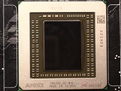
The Grenada silicon will have the same specs as Hawaii - 2,816 GCN stream processors, 176 TMUs, 64 ROPs, and a 512-bit wide GDDR5 memory interface, holding 4 GB memory. Refinements in the silicon over Hawaii could allow AMD to increase clock speeds, to outperform the GTX 980 and GTX 970. We don't expect the chip to be any more energy efficient at its final clocks, than Hawaii. AMD's design focus appears to be performance. AMD could save itself the embarrassment of a loud reference design cooler, by throwing the chip up for quiet custom-design cooling solutions from AIB (add-in board) partners from day-one.

Possible NVIDIA GM200 Specs Surface

Somebody sent our GPU-Z validation database a curious looking entry. Labeled "NVIDIA Quadro M6000" (not to be confused with AMD FirePro M6000), with a device ID of 10DE - 17F0, this card is running on existing Forceware 347.09 drivers, and features a BIOS string that's unlike anything we've seen. Could this be the fabled GM200/GM210 silicon?

The specs certainly look plausible - 3,072 CUDA cores, 50 percent more than those on the GM204; a staggering 96 ROPs, and a 384-bit wide GDDR5 memory interface, holding 12 GB of memory. The memory is clocked at 6.60 GHz (GDDR5-effective), belting out 317 GB/s of bandwidth. The usable bandwidth is higher than that, due to NVIDIA's new lossless texture compression algorithms. The core is running at gigahertz-scraping 988 MHz. The process node and die-size are values we manually program GPU-Z to show, since they're not things the drivers report (to GPU-Z). NVIDIA is planning to hold a presser on the 8th of January, along the sidelines of the 2015 International CES. We're expecting a big announcement (pun intended).

NVIDIA GeForce GTX TITAN II Detailed

Riding on the success of its GM204 silicon, it looks like NVIDIA won't wait for the 20 nm silicon fab process to build its next big GPU, which powers its enthusiast-segment graphics cards. The GM200 silicon will be built on the existing 28 nm silicon fab process. Among other SKUs, NVIDIA's next GeForce GTX TITAN product, the GTX TITAN II, could be based on this chip. A curious-looking data entry was submitted from an anonymous source to SiSoft's hardware database, which gives away some rather glaring details of the GM200.

To begin with, the GM200 will be built on the existing 28 nm node, and will feature a die-area of 551 mm². The chip will be based on the "Maxwell" architecture, and feature 3,072 CUDA cores, cushioned by a 3 MB L3 cache. The chip will likely feature a 384-bit wide GDDR5 memory interface, with lossless texture compression algorithms, which work to step up memory bandwidth. The standard memory amount is a staggering 12 GB, double that of the first-generation GTX TITAN. Given how AMD recently gave 8 GB variants of its Radeon R9 290X a coordinated launch, GPU vendors could be seeing a utility in giving their products such massive amounts of video memory, to cope with resolutions such as 4K Ultra HD, and perhaps even 5K 16xHD. The chip features reasonably high clock speeds, with the core running at 1100 MHz, and a staggering 1390 MHz GPU Boost. The memory, however, is clocked at 6.00 GHz.

NVIDIA Moving Around the Fabled GeForce GTX TITAN II

NVIDIA is moving around engineering samples of what it describes as "GM200 A1 graphics processor," in its shipping manifest. The sample was making its way from Taiwan, to Bangalore, India, from where it's likely pushed to the company's facilities in Bangalore and Hyderabad. A1 steppings of NVIDIA chips are usually pre-production, and bound for just a few more rounds of testing, before being upgraded to "A2" and mass-produced. German tech site 3DCenter.org also pulled out some likely specifications from its sources.

To begin with, the GM200, like the GM204, will be built on existing 28 nm silicon fabrication process, as both NVIDIA and AMD appear to have suffered design setbacks due to their common foundry partner, TSMC, not being able to set its next-gen 20 nm node up to speed in time. The GM200 is expected to feature over 4,000 CUDA cores, although the exact number is unknown. It is expected to widen the memory bus to 512-bit. Given the existing process, the GPU will be huge. Over 600 mm² huge. NVIDIA will probably bank on the energy efficiency of its "Maxwell" architecture to cope with thermal loads put out by a chip that big. The GM200-based "GeForce GTX TITAN II" could launch in the first half of 2015.

NVIDIA GM204 and GM206 to Tape-Out in April, Products to Launch in Q4?

It looks like things are going horribly wrong at TSMC, NVIDIA and AMD's principal foundry partner, with its 20 nm manufacturing process, which is throwing a wrench into the works at NVIDIA, forcing it to re-engineer an entire lineup of "Maxwell" GPUs based on existing 28 nm process. Either that, or NVIDIA is confident of delivering an efficiency leap using Maxwell on existing/mature 28 nm process, and saving costs in the process. NVIDIA is probably drawing comfort from the excellent energy-efficiency demonstrated by its Maxwell-based GeForce GTX 750 series. According to a 3DCenter.org report, NVIDIA's next mainline GPUs, the GM204 and GM206, which will be built on the 28 nm process, and "Maxwell" architecture, will tape out later this month. Products based on the two, however, can't be expected before Q4 2014, as late as December, or even as late as January 2015.

GM204 succeeds GK104 as the company's next workhorse performance-segment silicon, which could power graphics card SKUs ranging all the way from US $250 to $500. An older report suggests that it could feature as many as 3,200 CUDA cores. The GM204 could be taped out in April 2014, and the first GeForce products based on it could launch no sooner than December 2014. The GM206 is the company's next mid-range silicon, which succeeds GK106. It will tape out in April, alongside the GM204, but products based on it will launch only in January 2015. The GM200 is a different beast altogether. There's no mention of which process the chip will be based on, but it will succeed the GK110, and should offer performance increments worthy of being a successor. For that, it has to be based on the 20 nm process. It will tape-out in June 2014, and products based on it will launch only in or after Q2 2015.

GM107 Features 128 CUDA Cores Per Streaming Multiprocessor

NVIDIA's upcoming GM107 GPU, the first to be based on its next-generation "Maxwell" GPU architecture, reportedly features a different arrangement of CUDA cores and streaming multiprocessors to those typically associated with "Kepler," although the component hierarchy is similar. The chip reportedly features five streaming multiprocessors, highly integrated computation subunits of the GPU. NVIDIA is referring to these parts as "streaming multiprocessor (Maxwell)," or SMMs.

Further, each streaming multiprocessor features 128 CUDA cores, and not the 192 CUDA cores found in SMX units of "Kepler" GPUs. If true, GM107 features 640 CUDA cores, all of which will be enabled on the GeForce GTX 750 Ti. If NVIDIA is carving out the GTX 750 by disabling one of those streaming multiprocessors, its CUDA core count works out to be 512. NVIDIA will apparently build two GPUs on the existing 28 nm process, the GM107, and the smaller GM108; and three higher performing chips on the next-generation 20 nm process, the GM206, the GM204, and the GM200. The three, as you might have figured out, succeed the GK106, GK104, and GK110, respectively.
Return to Keyword Browsing
Apr 26th, 2024 21:47 EDT change timezone

New Forum Posts

Popular Reviews

Controversial News Posts