News Posts matching #GeForce GTX 470

Return to Keyword Browsing

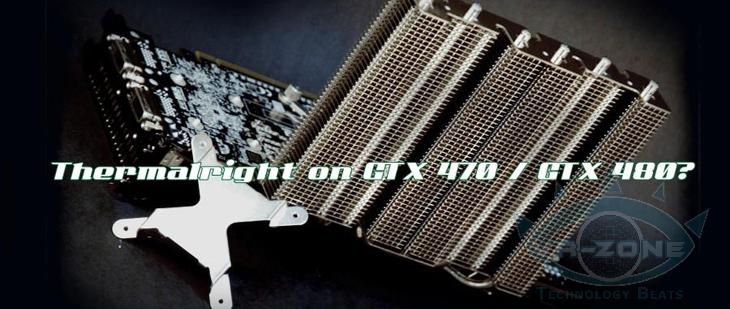
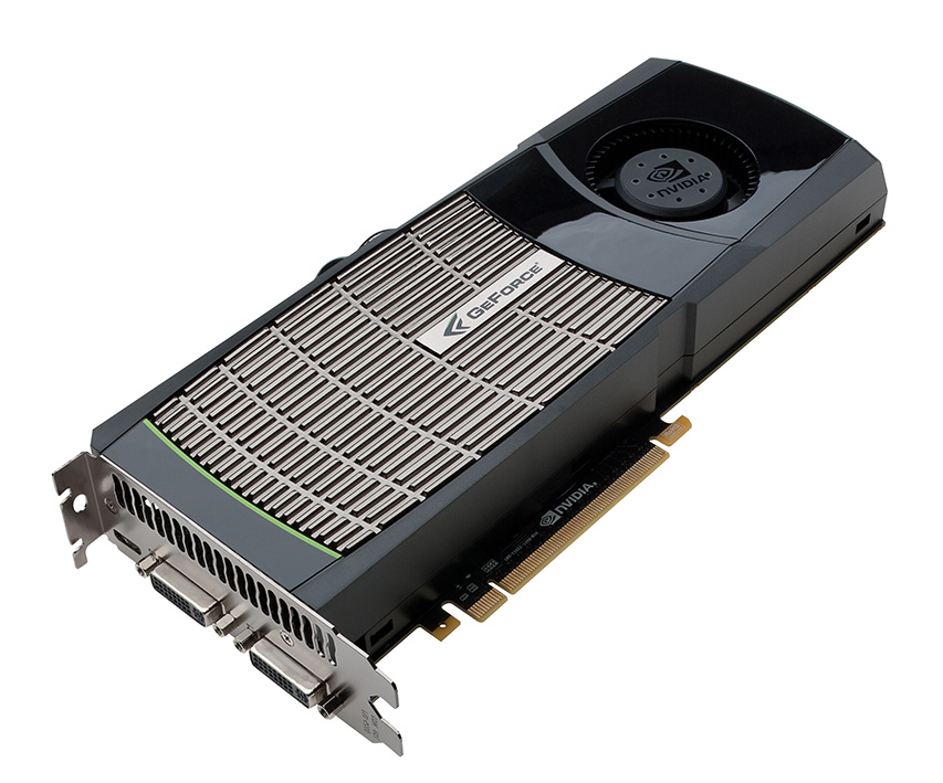
Inno3D Readies First ''Non-Reference'' GeForce GTX 470 Graphics Card

Inno3D seems to be in a bit of a hurry to bag the title of "first to come out with a non-reference GeForce GTX 400 graphics card," and is working tirelessly to get there. The company is readying a new "non-reference" graphics card, put in quotes because for the most part it is in fact a reference design. Traditionally, NVIDIA disallows its board partners from designing their own non-reference graphics cards based on newly-launched high-end GPUs, with a few concessions made for designs with factory-fitted water-blocks, or minor cosmetic changes, apart from letting their own sticker design, box design, bundle, and to an extant, pricing.

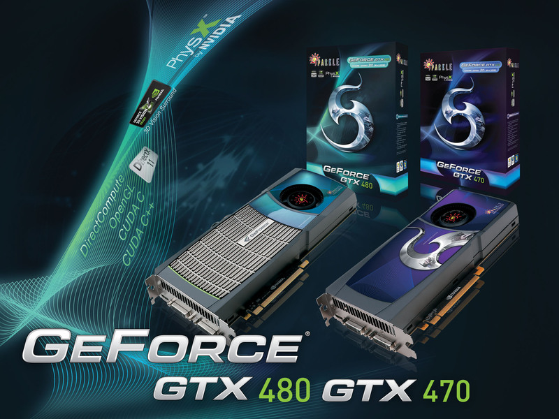
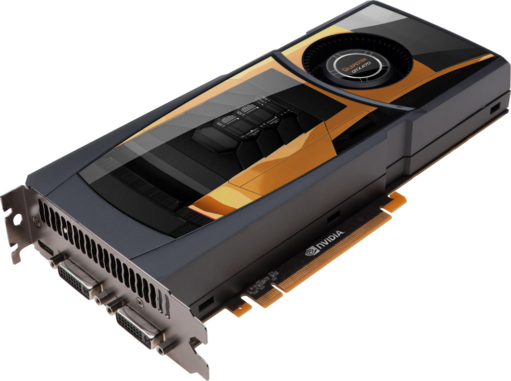
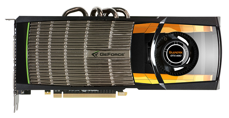
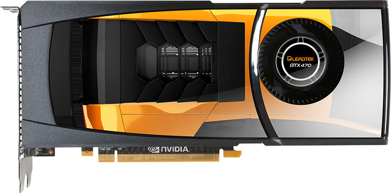
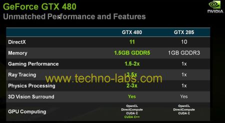
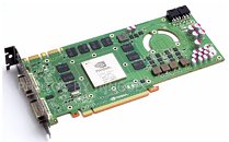
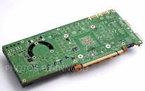
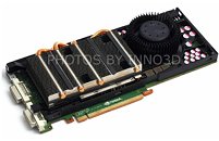
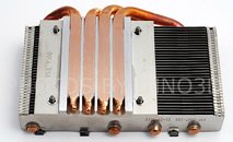
Inno3D's concession comes in the form of two things: 1. an NVIDIA reference-design PCB, which is now green instead of black, and 2. looking at the pictures, possibly a different cooler shroud design, although internally the cooling assembly remains reference design. Inno3D may roll out graphics cards with reference NVIDIA clock speeds, and also those with higher clock speeds. As with every other GTX 470 made so far, Inno3D's card is based on the GF100 GPU, it is DirectX 11 compliant, packs 448 CUDA cores, and 1.25 GB (1280 MB) of GDDR5 memory across a 320-bit wide interface. It supports 3-way SLI. At this point, there is no word on when exactly the card comes out, or pricing.

Thermalright Makes its Popular VGA Coolers Fermi-Ready

Thermalright is said to be working on a bolt-through kit (BTK), the GF 100 VGA BTK, that lets popular existing VGA heatsinks by the company to support the NVIDIA GF100 GPU, on GeForce GTX 480 and GeForce GTX 470 graphics cards. The Thermalright Spitfire, HR-03 GT and HR-03 GTX heatsinks will be able to make use of the new BTK. The company is also said to be working on two new VRM heatsinks that are tailor-made for the reference PCBs of the two cards, the VRM GTX 480, and VRM GTX 470. These allow existing users of the above three heatsinks, and people looking to buy them some future-proofing. The GF 100 VGA BTK, VRM GTX 480 and VRM GTX 470 will be released in the weeks to come.

SPARKLE Announces GeForce GTX 480/470 Graphics Accelerators

SPARKLE Computer Co., Ltd., the professional VGA card manufacturer and supplier, today proudly announced the SPARKLE GeForce GTX 480/470 Graphics Cards, which are the most powerful single chip graphics cards on the planet for gaming and beyond. Packing in 3 billion transistors, double the CUDA cores of previous generation GPUs, a high speed GDDR5 memory interface, and full DirectX 11 support, the SPARKLE GeForce GTX 480/470 Graphics Cards are designed for groundbreaking graphics performance. With a revolutionary new scalable geometry pipeline and enhanced anti-aliasing capabilities, the SPARKLE GeForce GTX 480/470 Graphics Cards are the world's most powerful single GPU graphics cards solution, delivering up to 3 times faster performance than previous GTX 285 single GPU solutions.

With the power of GF100 GPUs, the SPARKLE GeForce GTX 480/470 Graphics Cards bring ultimate DX11 HD gaming experience to high-end gamers. The SPARKLE GeForce GTX 480/470 Graphics Cards place gamers in the center of the action and experience true DirectX 11 gaming cinema in extreme HD (2560x1600) resolutions-all enabled by GF100's revolutionary compute architecture, NVIDIA 3-way SLI technology, and incredible performance in the latest DX11 games including Dirt 2, Stalker:OCP, Alien VS. Predator, Metro 2033 and so on. With 1.5~3 times more performance than prior generation GPUs, the SPARKLE GeForce GTX 480/470 Graphics Cards tear through complex DirectX 10 environments and cinematic effects at blazing frame rates in extreme HD resolutions.

ZOTAC Unleashes Next-Generation Graphics Cards

ZOTAC International, the world's largest manufacturer of graphics cards, motherboards and mini-PCs in the channel, today unleashes the world's most powerful graphics cards capable of delivering a phenomenal gaming experience and unmatched processing power - the new ZOTAC GeForce GTX 480 and GeForce GTX 470 graphics cards. The ZOTAC GeForce GTX 480 and GeForce GTX 470 graphics cards take gaming to uncharted levels with new Microsoft DirectX 11, 32x anti-aliasing, NVIDIA 3D Vision Surround and HDMI 1.3a technologies.

The new ZOTAC GeForce GTX 480 and GeForce GTX 470 deliver exceptional performance and visuals with an enhanced unified architecture that features hundreds of programmable unified shaders ready to process all GPU needs for extreme high-definition 3D gaming and everyday tasks. The unified architecture combines with a large 1536MB frame buffer on the ZOTAC GeForce GTX 480 and 1280MB frame buffer on the ZOTAC GeForce GTX 470 to deliver high-quality details and breathtaking performance.

EVGA Unleashes Full-Fledged Lineup of GeForce GTX 400 Series Graphics Cards

EVGA unleashed a lineup of graphics cards based on NVIDIA's new GeForce GTX 480 and GeForce GTX 470 graphics processors, complete with overclocked, overclocker-friendly, and water cooling-ready models. While the air-cooled models retain NVIDIA's reference design, the Hydro Copper series models sport a full-coverage, copper-rich water-block made for EVGA by Swiftech. On the air-cooled offer are base-models for the GTX 480 and GTX 470 that use NVIDIA reference clock-speeds, and level-1 overclock (Superclocked / SC) models. The level-3 overclock (For The Win / FTW) only come under the Hydro Copper series, with no air-cooled FTW models. Details follow:
  • EVGA GeForce GTX 480 (015-P3-1480-TR): 700/1401/924 MHz, reference air-cooled, US $499.99
  • EVGA GeForce GTX 480 SC (015-P3-1482-AR): 725/1450/950 MHz, reference air-cooled, US $529.99
  • EVGA GeForce GTX 480 FTW Hydro Copper (015-P3-1489-AR): 750/1500/950 MHz, Hydro Copper water-block pre-fitted, US $649.99
  • EVGA GeForce GTX 470 (012-P3-1470-TR): 607/1215/837 MHz, reference air-cooled, US $349.99
  • EVGA GeForce GTX 470 SC (012-P3-1472-AR): 625/1250/850 MHz, reference air-cooled, US $369.99
  • EVGA GeForce GTX 470 FTW Hydro Copper (012-P3-1479-AR): 650/1300/950 MHz, Hydro Copper water-block pre-fitted, US $499.99

NVIDIA Announces the GeForce GTX 480 and GeForce GTX 470 Graphics Cards

NVIDIA finally released the graphics cards it made many wait for: the DirectX 11 compliant GeForce GTX 480 and GeForce GTX 470. The two were unveiled at the PAX East gaming event, in the United States, as publications were allowed to post reviews right away. The two are based on the NVIDIA GF100 GPU, built on the 40 nm process. The higher-end GeForce GTX 480 packs 480 shader units (now referred to by NVIDIA as "CUDA cores"), branched geometry processing along with multiple tessellation units, and a 384-bit wide GDDR5 memory interface to connect to 1536 MB (1.5 GB) of memory.

The GeForce GTX 470 is the more affordable part, it packs 448 CUDA cores, and a 320-bit GDDR5 memory interface to connect to 1280 MB (1.25 GB) of memory. Both models support new features by NVIDIA, such as CUDA 3.0, faster PhysX acceleration, Stereoscopic 3D, 3D Vision surround multi display technology, as well as support for OpenCL and DirectCompute 5.0. While the GeForce GTX 480 has a suggested retail price of US $499, the GTX 470 is suggested to be priced at $349, although final pricing set by board partners could vary. NVIDIA is initially making tens of thousands of these cards, which should be available worldwide a little after April 12th.

Leadtek Ready with GeForce GTX 400 Series Graphics Cards

Leadteak is one of the many NVIDIA partners ready with its offering of GeForce GTX 470 and GeForce GTX 480 graphics cards, pictured ahead of its launch. As with every other GeForce 400 series SKU in the making, these cards stick to NVIDIA's reference design. The Leadtek GeForce GTX 480 is DirectX 11 compliant, has 480 CUDA cores, and 1536 MB of GDDR5 memory across a 384-bit memory interface, while the GeForce GTX 470 has 448 CUDA cores, and 1280 MB of GDDR5 memory across a 320-bit memory interface. Both are 3-way SLI capable. The two are expected to be launched later this week.

NVIDIA Claims Upper Hand in Tessellation Performance

A set of company slides leaked to the press reveals that NVIDIA is claiming the upper hand in tessellation performance. With this achievement, NVIDIA is looking to encourage leaps in geometric detail, probably in future games that make use of tessellation. NVIDIA's confidence comes from the way its GF100 GPU is designed (further explained here). Each GF100 GPU physically has 16 Polymorph Engines, one per streaming multiprocessor (SM) which helps in distributed, parallel geometry processing. Each Polymorph Engine has its own tessellation unit. With 15 SMs enabled on the GeForce GTX 480 and 14 on the GeForce GTX 470, there are that many independent tessellation units.

NVIDIA demonstrated its claims in the presentation using the Unigine Heaven, where the GeForce GTX 480 was pitted against a Radeon HD 5870. In many scenes where tessellation is lower, the GPUs performed neck-and-neck, with the GTX 480 performing better more often. But in scenes with heavy tessellation (particularly the "dragon" scene, where a highly detailed model of a dragon needs to be rendered with densely tessellated meshes, the GTX 480 clocks nearly a 100% performance increment over the HD 5870. NVIDIA has been confident about the tessellation performance back since January, when it detailed the GF100 architecture. The GeForce GTX 400 series graphics cards will be unveiled on the 26th of March.

Images Courtesy: Techno-Labs

XFX GeForce GTX 480 and GeForce GTX 470 Pictured

Here they are folks, pictures of the GeForce GTX 480 and GeForce GTX 470 complete with partner branding. These come from XFX, both sticking to NVIDIA's reference design. The XFX GeForce GTX 480 comes with the usual feature set of 1536 MB of GDDR5 memory, 480 CUDA cores, and a broad feature set that includes support for DirectX 11, CUDA, PhysX, 3D Vision Surround, and 3-way SLI. The GeForce GTX 470 retains this feature set, albeit with 448 CUDA cores, and 1280 MB of GDDR5 memory. The two will be released on the 26th of March.

GeForce GTX 400 Series Clock Speeds and Other Details Surface

Exactly a week ahead of releasing its GeForce GTX 400 series accelerators, NVIDIA held meetings with the press discussing the company's newest technologies, including GeForce GTX 400 series. Some lesser known details about the GeForce GTX 480 and GeForce GTX 470 surfaced, among more known and established ones. To begin with, the GeForce GTX 480 is confirmed to have a CUDA core (shader core) count of 480. The GF100 core operates at 700 MHz, its shader domain at 1401 MHz, and the memory operates at 924 MHz (actual, 1848 MHz DDR, 3700 MHz effective). With a GDDR5 memory bus width of 384-bit, the effective memory bandwidth would be 173.4 GB/s.

The GeForce GTX 470, on the other hand, has 448 CUDA cores, clock speeds of 607 MHz core, 1215 MHz shader domain, and 837 MHz memory (actual, 1674 MHz DDR, 3348 MHz effective). With a GDDR5 memory bus width of 320-bit, the effective memory bandwidth would be 130.7 GB/s. While the GTX 480 has a board power of 295W, the GTX 470 has a board power of 225W. Another piece of information the source reveals is that internal testing by NVIDIA showed that the performance level to expect from the GeForce GTX 470 should be 5-10% higher than that of the ATI Radeon HD 5850. The GeForce GTX 480 should be expected to be just that much faster than the ATI Radeon HD 5870. It is also expected that the target price of the GeForce GTX 480 should be typically US $499, while the GTX 470 should go typically for US $349. Detailed reviews of the two should be up by this time, next week.

GeForce GTX 480 has 480 CUDA Cores?

In several of its communications about Fermi as a GPGPU product (Next-Gen Tesla series) and GF100 GPU, NVIDIA mentioned the GF100 GPU to have 512 physical CUDA cores (shader units) on die. In the run up to the launch of GeForce 400 series however, it appears as if GeForce GTX 480, the higher-end part in the series will have only 480 of its 512 physical CUDA cores enabled, sources at Add-in Card manufacturers confirmed to Bright Side of News. This means that 15 out of 16 SMs will be enabled. It has a 384-bit GDDR5 memory interface holding 1536 MB of memory.

This could be seen as a move to keep the chip's TDP down and help with yields. It's unclear if this is a late change, because if it is, benchmark scores of the product could be different when it's finally reviewed upon launch. The publication believes that while the GeForce GTX 480 targets a price point around $449-499, while the GeForce GTX 470 is expected to be priced $299-$349. The GeForce GTX 470 has 448 CUDA cores and a 320-bit GDDR5 memory interface holding 1280 MB of memory. In another report by Donanim Haber, the TDP of the GeForce GTX 480 is expected to be 298W, with GeForce GTX 470 at 225W. NVIDIA will unveil the two on the 26th of March.

GeForce 196.78 Beta Driver Runs GeForce GTX 470

Czech technology website PCTuning confirmed a few details about NVIDIA's upcoming performance graphics accelerator, the GeForce GTX 470. It was found out that a beta driver by NVIDIA, GeForce 196.78 supports GeForce 400 series accelerators, and was able run a qualification sample of GeForce GTX 470. The card was using A3 revision GF100 silicon. The driver's System Information dialog revealed that the card indeed has 448 CUDA cores (SIMD units). Further, it has 1280 MB of memory, and a 320-bit wide memory interface. NVIDIA also changed the way it represents memory clock speeds. Since it is using GDDR5 memory, while the memory has an actual clock speed of 1000 MHz, the data rate (DDR speed) is represented first, as 2000 MHz, and "effective speed" next, which is 4000 MHz.

Given these speeds, at 1000 MHz GDDR5, the GPU has a memory bandwidth of 160 GB/s. Without compromise on looks and quality, NVIDIA kept the cooler design basic. It has a matte finish. Display outputs include two DVI-D, and one mini HDMI. It supports NVIDIA 3D Vision Surround (a technology competitive to ATI Eyefinity, to span a display head across multiple physical displays), just that NVIDIA requires at least two accelerators in SLI to use it. NVIDIA's GeForce 400 series graphics accelerators will be launched on the 26th of this month.

GeForce GTX 470 PCB and Cooler Pictured, Too

A couple of days after pictures of the PCB and cooling assembly of the GeForce GTX 480 made it to the internet, fresh pictures emerged, this time of the GeForce GTX 470, the slightly toned-down part in the GeForce 400 series. The GTX 470, like the GTX 480, is based on NVIDIA's GF100 core. The reference design PCB is certainly shorter than that of the GTX 480, and compacts its resources. Since the GTX 470 has a 320-bit wide memory interface, it makes do with 10 memory chips, seen surrounding the GPU from three sides. A simpler VRM is used: 4-phase vGPU and 1-phase vMem. Power is drawn in from two 6-pin power connectors.

The fan connects over its usual 4-pin PWM-controlled line. Some smart compacting of components made space for two intakes to be cut out, which help the blower draw in some fresh air. The cooling assembly, again is compacted accordingly. Since these new pictures are more clear, we can see that the area over the GPU isn't devoid of a copper surface as earlier thought. In fact, as some community members observed, it is a base with copper heatpipes making direct contact with the GPU. The cooler has protrusions at the right spots to make contact with memory chips and MOSFETs. The GTX 470 is slated to be the more affordable of the GTX 400 series, which will be unveiled on March 26. Follow the source link for equally good quality photography of the GTX 480's PCB.

GeForce GTX 470 Graphics Card Pictured

A picture of what NVIDIA's reference design for its next-gen performance graphics card, the GeForce GTX 470, could look like made it to sections of the media. The card is characteristically shorter than the GTX 480 reference design card spotted earlier. The GeForce GTX 470 will be the slightly more affordable part in the series. It is based on NVIDIA's new GF100 graphics core. The GTX 470 has 448 CUDA cores (shader cores), and has a 320-bit wide GDDR5 memory interface. Board partners will sell these cards with 1280 MB of memory. The back of the card shows tracks for 10 memory chips (confirming the 320-bit wide memory interface), and interestingly, also lacks traces for an external display IO processor (like the NVIO2 processor on GT200 based accelerators), cutting down the overall cost of manufacturing. The card draws power from two 6-pin power connectors, and has two SLI fingers for 3-way SLI support. Its connectivity includes two DVI-D, and HDMI.

GeForce GTX 400 Series Performance Expectations Hit the Web

A little earlier this month, NVIDIA tweeted that it would formally unveil the GeForce GTX 400 series graphics cards, NVIDIA's DirectX 11 generation GPUs, at the PAX East gaming event in Boston (MA), United States, on the 26th of March. That's a little under a month's time from now. In its run up, sources that have access to samples of the graphics cards seem to be drawing their "performance expectations" among other details tricking in.

Both the GeForce GTX 480 and GTX 470 graphics cards are based on NVIDIA's GF100 silicon, which physically packs 512 CUDA cores, 16 geometry units, 64 TMUs, 48 ROPs, and a 384-bit GDDR5 memory interface. While the GTX 480 is a full-featured part, the GTX 470 is slightly watered-down, with probably 448 or 480 CUDA cores enabled, and a slightly narrower memory interface, probably 320-bit GDDR5. Sources tell DonanimHaber that the GeForce GTX 470 performs somewhere between the ATI Radeon HD 5850 and Radeon HD 5870. This part is said to have a power draw of 300W. The GeForce GTX 480, on the other hand, is expected to perform on-par with the GeForce GTX 295 - at least in existing (present-generation) applications. A recent listing by an online store for a pre-order, put the GTX 480 at US $699.
Return to Keyword Browsing
Apr 27th, 2024 00:49 EDT change timezone

New Forum Posts

Popular Reviews

Controversial News Posts