News Posts matching #Goldmont Plus

Return to Keyword Browsing

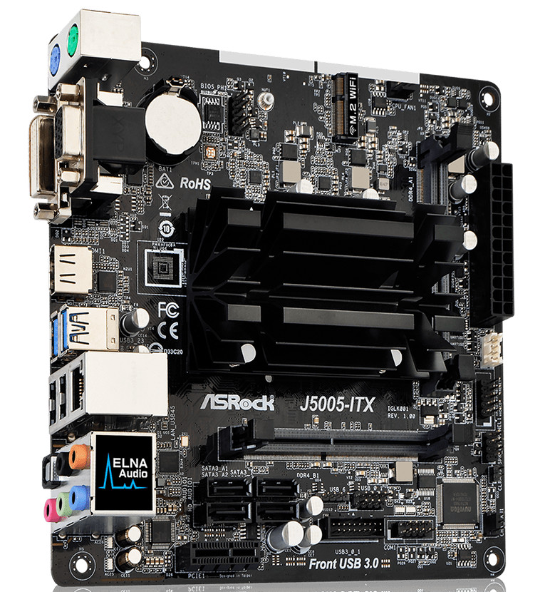
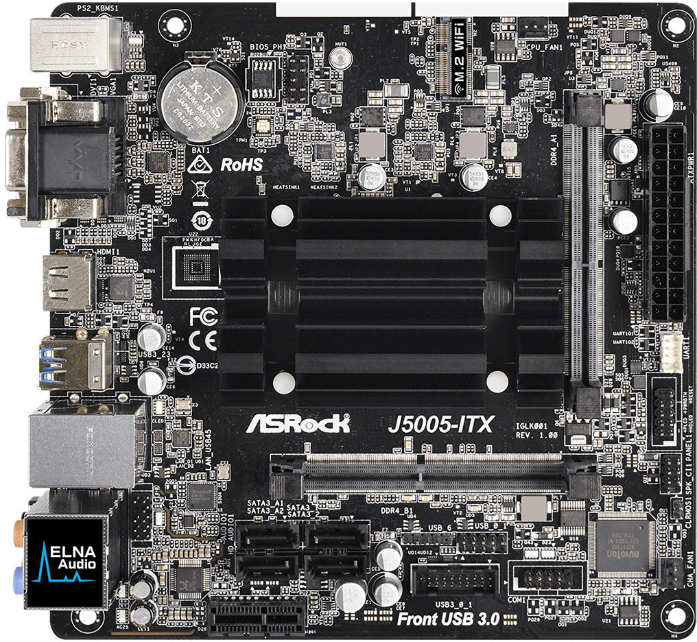
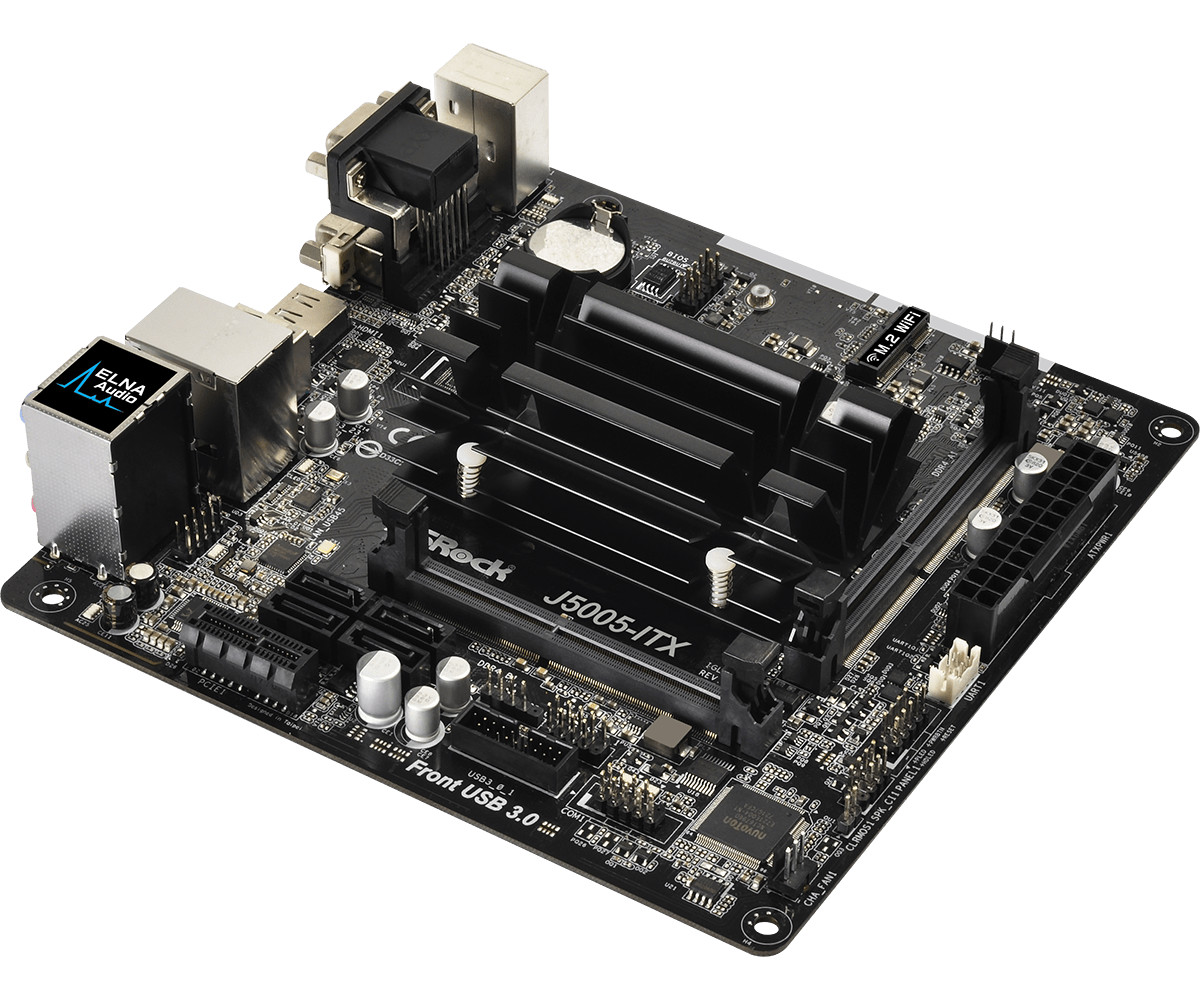
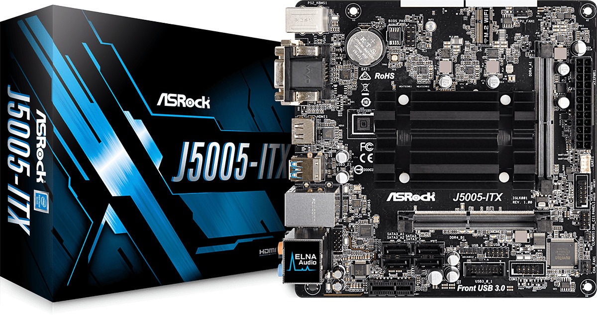
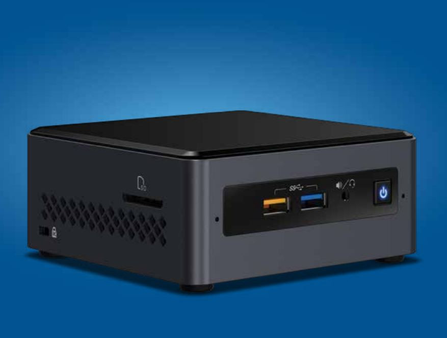
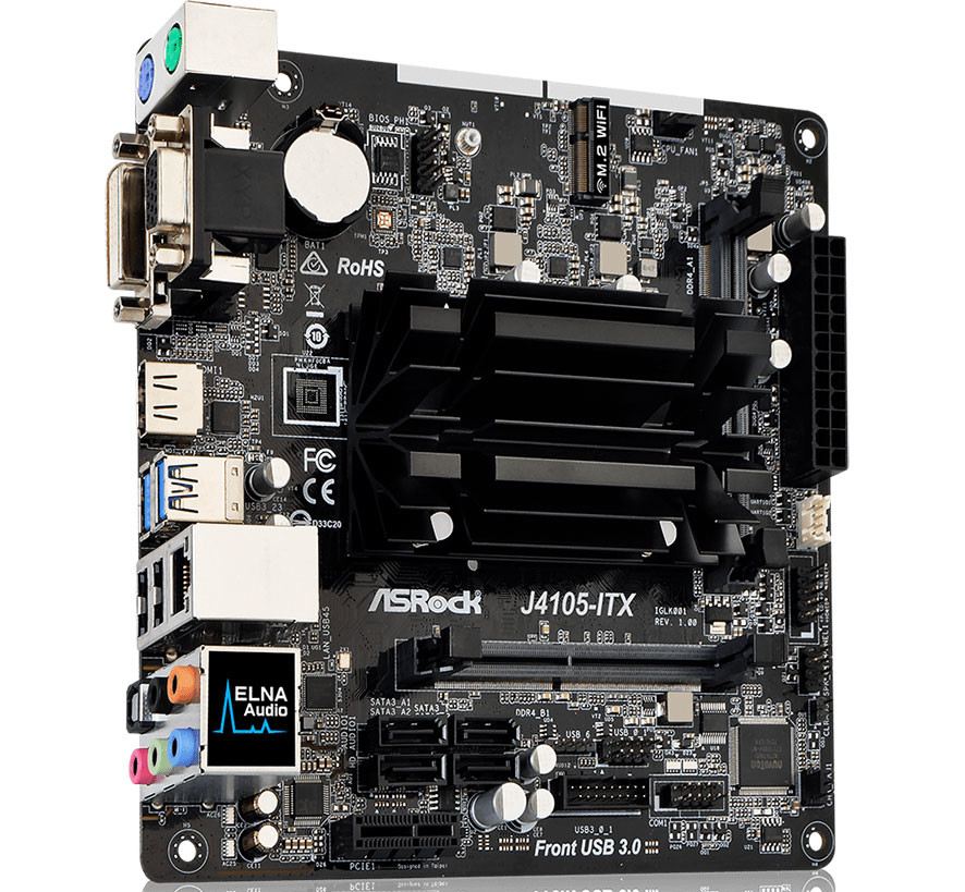
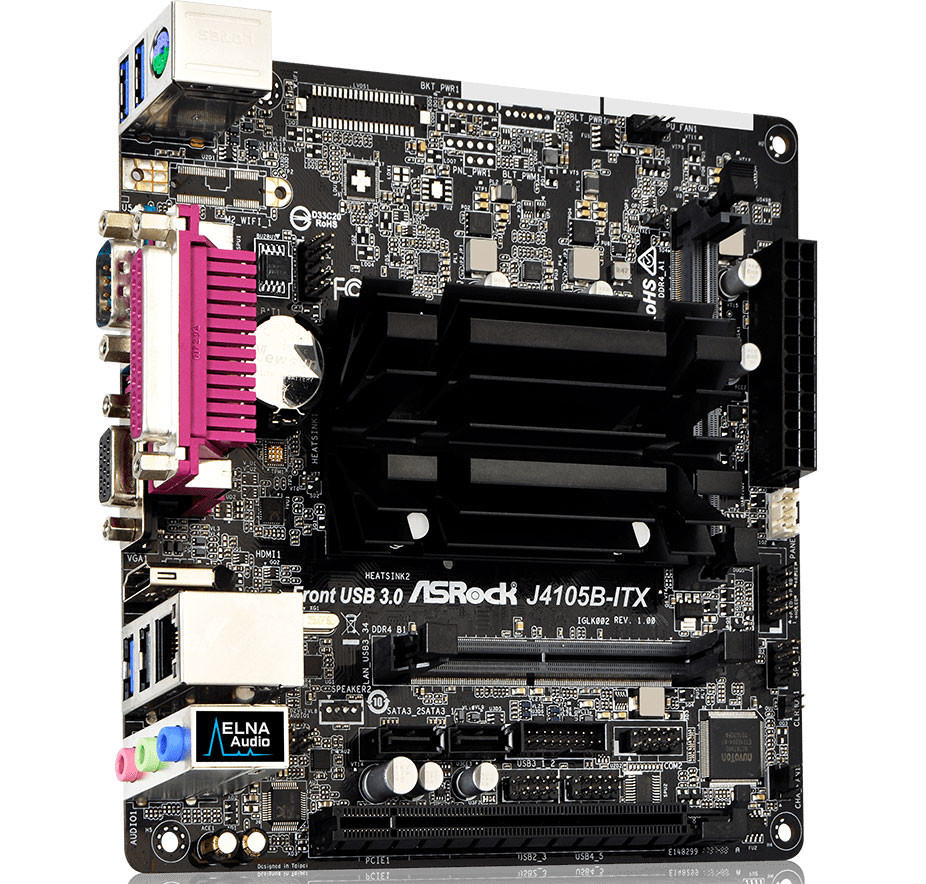
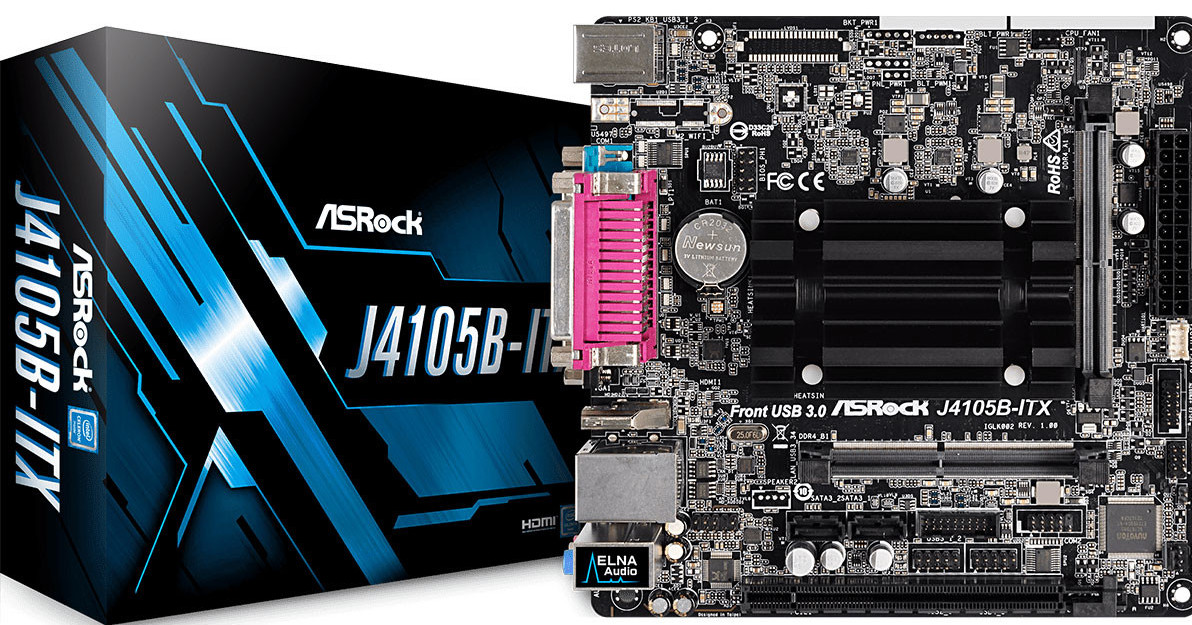
Intel Gemini Lake Refresh Reaches End of Life

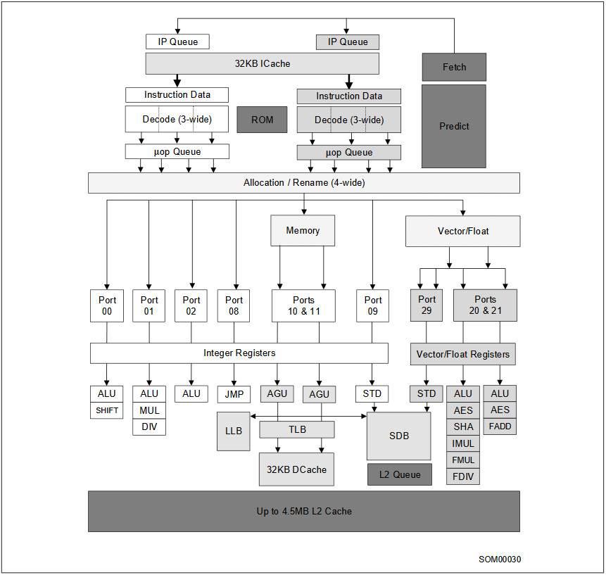
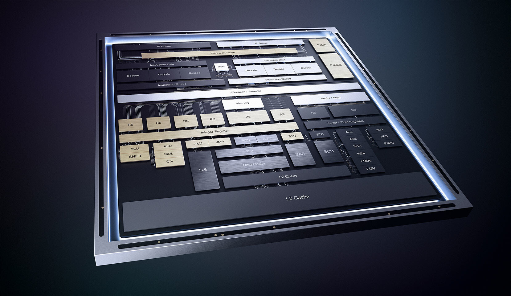
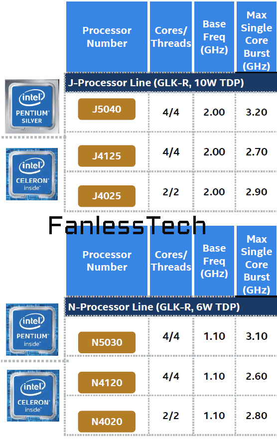
Intel has posted two product change notifications regarding the Gemini Lake Refresh, which is now reaching the end of its life. Launched in 2019 as a refresh to the original Gemini Lake, these low-end products had a longer lifespan than the original Gemini Lake (2017-2020). Most commonly found on low-end PCs, AIOs, and Mini PCs, these Gemini Lake Refresh CPUs were based on the 14 nm Goldmont Plus microarchitecture. Coming with up to four cores without HyperThreading, these CPUs were ideal for lower-power applications as their TDP was rated between 6-10 Watts.

Intel has separated the product change into two categories, with the first consisting of Celeron N4120, Celeron 4020, and Pentium Silver N5030, while the other features Celeron J4025, Pentium Silver J5040, Celeron N4020C, and Celeron J4125. Intel will ship the first group of CPUs by May 24, 2024, and the second by February 23, 2024. The last round of orders will go out by November 24, 2023, and August 25, 2023, respectively.

Intel Updates x86/x64 Software Developer Manual With Tremont Architecture Details

Intel has today released the 43rd edition of its x86/x64 ISA developer manual designed to help developers see what's new in x86 world and make software optimizations for Intel's platform. In the latest edition of the manual, Intel has revealed the details of its low-power x86 "Tremont" architecture designed for 10 nm efficient, low-power computing. Announced last year in October, Intel promised to deliver a big IPC increase compared to the previous generation low-power CPU microarchitecture like the Goldmont Plus family. To achieve extra performance, Intel has implemented a lot of new solutions.

For starters, Tremont boasts better branch prediction unit, with increased capacity for instruction queue and better path-based conditional and indirect prediction. The front-end fetch and decode pipeline have been updated as well. Now the design is a 6-wide Out of Order Execution (OoOE) pipeline which can process 6 instructions per cycle. The Data cache is now upgraded to 32 KB. The load and store execution pipelines are now doubled and they are capable of two loads and two stores, or one load and one store, depending on the application. Tremont also updates on one important point and that is a dedicated store data port for integer and vector integer/floating-point data. Another big improvement is happening in the cryptography department. Tremont now features Galois-field instructions labeled as the GFNI family of instructions. There are two AES units for faster AES encryption and decryption. The already implemented SHA-NI cryptography standard was enhanced and it now is much faster as well. For mode in-depth report please check out Intel's x86/x64 manual.
Intel Tremont

Intel Gemini Lake Refresh Coming This November

Intel is preparing to debut its next generation Pentium Silver and Celeron "Gemini Lake Refresh" low-power processors in November 2019. The latest company roadmap slide detailing low-power SoC rollout, sourced by FanlessTech, pinned their launch sometime between week 45-47 (November). These are two key variants of this silicon, J and N. The J variant targets low-power desktops and AIOs, while the N variant targets notebooks, tablets, and other portables.

"Gemini Lake Refresh" SoCs are built on Intel's latest 14 nm node, and pack up to four "Goldmont Plus" CPU cores, and the same Intel UHD graphics, but offer significantly higher clock-speeds on both the CPU cores and the iGPU. Leading the pack is the Pentium Silver J5040, clocked at 2.00 GHz with up to 3.20 GHz boost. This chip succeeds the J5005, which ticks at 1.50 GHz with 2.80 GHz boost. The table below details the other J and N series models with the clock-speeds and core-counts.

Intel "Tremont" Low-power CPU to Feature L3 Cache

Intel's next-generation Pentium Silver "Snow Ridge" SoC, featuring "Tremont" CPU cores, could see the debut of an L3 cache to the segment. Intel CPU cores in this segment, such as the "Goldmont Plus," only feature shared L2 caches across 4-core modules. The introduction of L3 cache was indicated by a new performance counter "MEM_LOAD_UOPS_RETIRED_L3_HIT," with a description clearly mentioning a "level 3 cache." The introduction of L3 cache as the SoC's LLC (last level cache) could mean Intel is trying to improve inter-component communication by introducting the L3 cache as "town-square" for the various components of the SoC, such as the CPU cores, the iGPU, and the integrated chipset. The company could deploy a ring-bus interconnect that has ring-stops at the various components, and slices of this L3 cache. Intel is building the "Snow Ridge" silicon on its swanky new 10 nm silicon fabrication process, and the chip could see a 2020 debut targeting network infrastructure devices.

Intel's Next Atom Core, Tremont, Revealed - Likely to Be Fabbed on the 10 nm Process

Intel, via its internal documentation that is, routinely, the source of new information on unreleased products, has revealed their next low-power architecture. Codenamed Tremont, the new architecture is expected to be developed on the company's 10 nm process (not unlike Ice Lake) and bring some performance improvements to the company's options for the embedded market.

Tremont will thus replace Intel's Goldmont Plus, which is still being manufactured on the company's 14 nm process (it hasn't been side-graded to the company's 14 nm + or ++ processes, due to these being less suited for denser chip designs). The new architecture will likely receive some specific performance improvements that mirror some of Intel's Core architecture's improvements, alongside support for new instruction sets - CLWB, GFNI (SSE-based), ENCLV, Split Lock Detection instruction set extensions are all extensions that will also be introduced in the company's Ice Lake cores, which increases the likelihood of the same process. Other functions introduced specifically for Tremont include CLDEMOTE, direct store, and user wait instructions.

ASRock Intros J5005-ITX Motherboard

While most Intel "Gemini Lake" SoC desktop motherboards are based on the cheaper Celeron J4005, a rare few, such as the ASRock J5005-ITX, implement the pricier Pentium Silver J5005 chip. What sets the J5005 apart from the J4005 is its quad-core "Goldmont Plus" CPU, and faster UHD Graphics 605 iGPU with higher clocks; which make the chip around 1.5 times pricier. Designed for machines with internal PSUs, the board draws power from a 24-pin ATX connector. A simple 2-phase VRM powers the 10W TDP SoC, and an aluminium heatsink keeps it cool.

The SoC is flanked by two DDR4 SO-DIMM slots, supporting up to 8 GB of memory. Expansion slots include a PCI-Express x1, and an M.2 E-key slot meant for WLAN cards. Display outputs include HDMI 2.0, D-Sub, and DVI. Four USB 3.0 ports (two on the rear panel, two by headers), gigabit Ethernet, and 8-channel HD audio, make for the rest of it. The board appears to be targeted at HTPC builders, as the UHD Graphics 605 appears sufficient for 4K UHD entertainment (10-bit HEVC encode/decode hardware acceleration). Given the $160 price of the SoC itself, we expect this board to be priced in the $200-250 range.

Intel Intros Two New NUCs Based on "Gemini Lake" SoCs

Intel today released two new barebones NUCs based on its latest "Gemini Lake" Pentium Silver and Celeron SoCs, the NUC 7 PJYH, and the NUC 7 CJYH. As their names might suggest, the PJYH is based on Pentium Silver J5005, while the CJYH implements Celeron J4005. The Pentium Silver J5005 packs a "Goldmont Plus" quad-core CPU clocked at 2.80 GHz, 4 MB of cache, and UHD Graphics 605 iGPU, while the Celeron J4005 features a dual-core "Goldmont Plus" CPU clocked up to 2.70 GHz, 4 MB cache, and UHD Graphics 600 iGPU.

As a barebones NUC, you're supposed to add your own memory, populating its two DDR4 SO-DIMM slots (up to 8 GB), and a 2.5-inch SSD or HDD. Networking connectivity includes 802.11ac WLAN, Bluetooth 5.0, and gigabit Ethernet. Display outputs include two HDMI ports. USB connectivity includes two each of USB 3.0 and USB 2.0, from which one of the front USB 3.0 ports (yellow) has high-current (10A). There's also an SD card slot. A 65W power-brick runs the NUC. The two could be priced in the range of $299-$399.

ASRock Intros a Pair of Celeron "Gemini Lake" ITX Motherboards

ASRock introduced a pair of mini-ITX desktop motherboards implementing Intel's new Celeron "Gemini Lake" SoCs. The ASRock J4105-ITX and J4105B-ITX, as their names suggest, are powered by Celeron J4105 "Gemini Lake" SoCs, which combine a quad-core "Goldmont Plus" CPU ticking at 2.50 GHz, with new Intel UHD 600 Graphics. The integrated graphics features hardware-acceleration of 10bpc HEVC video encoding and decoding in addition to new DRM standards, which should enable Netflix 4K, and other on-demand video services at 4K UHD resolution. The J4105-ITX and J4105B-ITX are similar, but for the latter featuring legacy connectivity such as LPT and RS232 COM ports, replacing 8-channel HD audio with 6-channel, and a DVI port. While the former has a PCIe x1 slot, the latter has an x16 slot with x2 wiring.

The board draws power from a 24-pin ATX connector. The SoC is cooled by a fan-less heatsink, and is wired to DDR4 SO-DIMM slots, supporting up to 8 GB of dual-channel DDR4-2400 memory. The 22 mm M.2 slot that has x1 wiring, is recommended only for a WLAN card. Storage connectivity includes four SATA 6 Gbps ports on the J4105-ITX, and two ports on the J4105B-ITX. Both boards come with gigabit Ethernet. Display outputs include DVI, HDMI, and D-Sub on the J4105-ITX; while the J4105B-ITX features D-Sub and HDMI. Both boards are expected to be priced around $170, given that the SoC itself costs $107.

Intel "Gemini Lake" SoC Graphics Supports 10-bit VP9 Hardware Decoding

Intel's upcoming Celeron and Pentium "Gemini Lake" SoCs feature not just faster CPU cores, but also a more feature-updated integrated graphics core. In a change-log entry made by Intel for a Linux kernel patch; the company describes hardware decoding support for 10-bit (1.07 billion-color) video formats, such as VP9. The integrated graphics now supports hardware decoding of VP9 10-bit Profile2. Its predecessor, "Apollo Lake," only supported hardware decoding up to VP9 8-bit Profile0. The change-log entry reads "Add support for Gemini Lake (aka. GLK) - Decoding: H.264/MPEG-2/VC-1/JPEG/VP8/HEVC/HEVC 10-bit/VP9/VP9 10-bit."

Intel "Gemini Lake" Low-power Architecture Features Wider Instruction Decode

Intel "Gemini Lake," the upcoming low-power x86 CPU micro-architecture which succeeds "Apollo Lake," will feature a wider 4-way decode unit, according to WikiChip, citing an Intel kernel patch, which mentions "Goldmont Plus has 4-wide pipeline for Topdown." The unit is now 33% wider than that of the "Apollo Lake" architecture, and double that of its predecessor, "Braswell." The new "Gemini Lake" CPU cores will be part of a new lines of Celeron and Pentium "Goldmont Plus" SoCs for low-power desktops, convertible notebooks, and tablets.
Return to Keyword Browsing
Apr 16th, 2024 00:52 EDT change timezone

New Forum Posts

Popular Reviews

Controversial News Posts