News Posts matching #HBM3

Return to Keyword Browsing

CXMT to Start HBM3E Mass Production by the End of 2026

CXMT is expected to start mass production of its first-ever HBM memory in the HBM3E form factor. According to an exclusive report from Reuters, this mass production is anticipated to begin within the next two months, meaning CXMT will officially start by the end of the year. Back in August, CXMT began risk production of HBM3E memory. However, the company has struggled with the yield of HBM3E memory modules, and this situation remains similar today, according to the latest report. While we don't have specific performance details, JEDEC's official data for HBM3E indicates a 1,024-bit width and speeds ranging from 9.2 Gbps per pin to 12.4 Gbps, with most standard configurations targeting 9.6 Gbps per pin. The total bandwidth is around 1.2 TB/s, and capacities range from 24 GB using 8-high stacks to 36 GB using 12-high stacks of 24 Gb layers.

CXMT's main challenge lies in the immaturity of the through-silicon via (TSV) technology it employs. In front-end manufacturing, CXMT achieves around 30% yields, while back-end processing adds about 70% on top of the original 30%. For example, Samsung uses about 5,000 TSVs per layer on HBM2, and SK hynix uses more than 8,000 TSVs per layer on its HBM3. However, data suggests that CXMT is attempting to achieve HBM3E with only 3,000 TSVs per layer and is trying to pack 8 layers into the regular 8-high HBM3E configuration. Given these challenges, the company is unlikely to transition to a higher-capacity 12-high HBM in the near term as it addresses engineering issues.

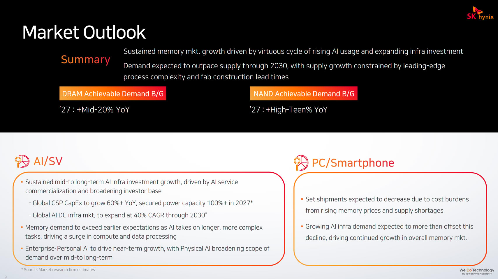
SK hynix Expects Memory Demand to Outpace Supply Through 2030

SK hynix reported its latest Q3 2026 quarterly results with a record $78.129 billion in net revenue. However, the company also shared a market outlook, highlighting its long-term supply agreements and plans for expansion with new fab capacity and facilities under construction. For the consumer market, the outlook is grim as SK hynix expects memory demand to continue outpacing supply through 2030. The main supply constraint is the complexity of leading-edge semiconductor nodes and the lengthy lead times for fab construction, which take years to translate into regular mass production volumes.

Despite sustained demand, pricing is also on an upward trajectory, with the average selling price of memory modules in Q3 increasing by over 20% compared to Q2. This is concerning, as it suggests that the prices of consumer electronics devices might jump by more than 20% once memory inventory is depleted. Although SK hynix expects a decrease in PC and smartphone shipments, this will be offset by a strong rollout of AI data centers. About 14 major customers, including most hyperscalers, have signed 5-year long-term agreements, which will account for over 50% of total capacity sold for 2027 and 2028.

Samsung HBM4E Passes Testing for NVIDIA's "Rubin Ultra" GPU

Samsung's upcoming HBM4E memory has reportedly passed testing for NVIDIA's next-generation "Rubin Ultra" AI GPU accelerator family. This is great news for the company, as its previous HBM3E didn't meet NVIDIA's requirements, leading NVIDIA to choose Samsung for GDDR7 only, instead of HBM3E. The new HBM generation brings significant advancements, and Samsung is one of the leading manufacturers with designs currently running at 14 Gbps per pin and 2,048 pins per HBM4E stack. Samsung can achieve a maximum bandwidth of 3.6 TB/s, and at 16 Gbps, this maximum memory bandwidth will increase to 4 TB/s for a single HBM4E stack.

With about a dozen memory stacks per AI accelerator or GPU, the total memory bandwidth will be remarkable. The company is currently offering this memory in a 12-layer (or 12-high) configuration with a memory density of 48 GB per stack. However, customer requirements will also include 8-layer 32 GB and 16-layer 64 GB stacks in the future.

SK hynix Reportedly Faces Difficulties in HBM Hybrid Bonding, Trailing Samsung

According to a process development engineer at SK hynix's future technology research institute, who spoke with Damnang, SK hynix is reportedly facing challenges in developing hybrid bonding technology for its HBM memory. These issues are significant enough that SK hynix has not yet begun production of samples, while Samsung has reportedly already sent out samples of HBM manufactured using hybrid bonding to customers. If true, this represents a major setback for SK hynix, whose HBM has held the top spot in global market share by revenue. This could potentially lead to a loss of market share among customers who require higher capacities, better performance, and more advanced technology from their HBM suppliers.

For those unfamiliar, hybrid bonding creates a permanent bond between two silicon chips using embedded metal bumps that are fused together to form a single chip. Multiple dies or entire silicon wafers can be connected by stacking the back ends of two chips together. This technology eliminates traditional chip bumps and directly bonds copper interconnections between the two chips. Essentially, hybrid bonding can create shorter distances, reducing latency and improving performance, lowering signal distortion, and offering many other benefits.

Samsung Foundry to Manufacture Anthropic AI ASIC on 2 nm Node

Samsung Foundry may be on the verge of securing a significant deal with AI lab Anthropic to manufacture AI accelerators. According to the latest report, Anthropic is developing its custom AI accelerator on Samsung's SF2 2 nm node, which will initially be produced in a lower volume of around 200,000 chips. The design and implementation of this ASIC are being handled by Broadcom, targeting around 4,000 TOPS of INT8 compute, with a TDP of 1,300 W per chip. This will be supported by either 192 GB of HBM3E or even 288 GB of HBM3E, if the design allows. The current production volume is low, as ASIC projects are typically counted in millions of chips. However, Anthropic is likely evaluating the project's viability, which requires a complete custom infrastructure with networking, rack design, power supply, cooling, and many other factors.

The current Samsung SF2 node is built using Low-NA EUV lithography and is manufactured in South Korea, with a new facility soon to be established in Taylor, Texas. For packaging these chips and integrating them with HBM, Samsung is likely to employ its I-Cube technology, which rivals TSMC's CoWoS and allows for 2.5D packaging. Combined with the 2 nm dies, Samsung can position itself as a serious manufacturing plant for external customers and slightly close the gap with TSMC and its contract manufacturing business.

Samsung to Double HBM4 and HBM4E Capacity in 2027 Amid Strong Demand

Samsung is reportedly increasing its orders for materials to boost high-bandwidth memory (HBM) production, with plans to double the production capacity of its current HBM4 and HBM4E manufacturing by 2027. According to SE Daily, the manufacturing capacity for HBM4 and HBM4E is expected to grow from around 20,000 wafers per month in 2026 to 50,000 wafers per month in 2027. This data is derived from the use of glass carriers, which are temporary glass panels placed over thin DRAM wafers to prevent warping or breaking as they are prepared for packaging. Since HBM involves stacking many thin DRAM modules, glass carriers stabilize these wafers until the packaging process begins and the glass is removed. As the unit is one glass carrier per wafer, this provides an estimate of how many HBM4 and HBM4E wafers are produced each month.

Additionally, Samsung's overall HBM production, which includes older generations like HBM3 and HBM3E, currently averages around 180,000 wafers this year and is expected to grow to about 250,000 HBM wafers next year, with 80% dedicated to HBM4 and HBM4E. Samsung began mass production of HBM4 on its sixth-generation 10 nm-class 1c node in February, with HBM4E customer samples available by mid-2026. Future production increases will focus on HBM4 and HBM4E, as customers seek higher densities and bandwidth for their AI accelerators.

CXMT Reportedly Struggles With HBM3E, Yields Are Only 25%

Chinese memory giant CXMT is reportedly facing difficulties with HBM3 production, according to South Korean media. Late last month, it was revealed that CXMT had begun risk production of HBM3E memory, lagging two generations behind Samsung, SK hynix, and Micron, who are already progressing with HBM4E sampling. At that time, it was known that the company was conducting HBM3E risk production in limited runs, but details were scarce. However, today we learn that three out of four HBM3E stacks are defective, indicating that CXMT currently operates at a 25% yield. Stacking DRAM is a complex task, as the technology required is much more intricate than planar DRAM manufacturing, an area where CXMT reportedly excels.

The low yields are reportedly due to the immaturity of the through-silicon via (TSV) technology that CXMT employs. In front-end manufacturing, CXMT achieves around 30% yields, while back-end processing yields about 70% on top of the original 30%. For instance, Samsung uses about 5,000 TSVs per layer on HBM2, and SK hynix uses more than 8,000 TSVs per layer on its HBM3. However, data suggests that CXMT is attempting to achieve HBM3E with only 3,000 TSVs per layer and is trying to pack 8 layers in the regular 8-Hi HBM3E configuration. Given these challenges, the company is unlikely to transition to a higher-capacity 12-Hi HBM in the near term as it addresses engineering challenges.

SK hynix Boosts Leading-Edge 1c DRAM Production to a Dominant Position

SK hynix is shifting much of its capacity to the latest 1c DRAM node, according to recent reports. The South Korean giant is transitioning the bulk of its memory production between nodes, and as DRAM technology advances, the company is moving its production to more advanced 10 nm-class nodes. For SK hynix, the sixth-generation 10 nm class 1c DRAM node accounted for 10% of production in Q1 2026, with an increase to about 13% in Q2. In the current third quarter, the company is expected to manufacture 24% of its DRAM on 1c, while Q4 will see more than a third (34%) produced on that node. By Q1 2027, the 1c node will account for around 35%, making the fifth-generation 10 nm-class 1b node at 33%, officially SK hynix's most dominant node.

As a reminder, DRAM nodes are not the same as conventional logic nodes. DRAM manufacturers use variations of 10 nm and scale them with more EUV layers or advanced features. For SK hynix, the currently dominant 1b node is around 12-13 nm in actual design and involves about 4 layers of EUV patterning, while the most advanced 1c node shrinks to 11-12 nm with 5-6 layers of EUV. SK hynix will use the 1c node to manufacture HBM4E, LPDDR6, and DDR5 memory. For the older 1b node, SK hynix produces DDR5, LPDDR5X, HBM3E, and HBM4.

DRAM Industry Revenue Rises 59.5% QoQ in 2Q26 as Supply Expansion Continues to Lag Demand Growth

TrendForce's latest findings on the memory industry reveal that sharp rises in traditional DRAM contract prices have led to a 59.5% QoQ increase in total DRAM industry revenue, reaching nearly US$154.73 billion in 2Q26.

Growing demand for AI servers, fueled by expanding LLM training and AI inference, has driven higher shipments of HBM3e, LPDDR5X, and high-capacity RDIMMS. The surge in agentic AI applications is further boosting RDIMM demand across various capacities.

CXMT Captures 10% of the Global DRAM Market Revenue Share

According to Counterpoint Research trackers, Chinese memory giant CXMT captured 10% of the global DRAM market share by revenue in Q2 2026, which is 150% more than the company had a year ago. On a quarterly basis, the company also experienced significant growth of 25%, as it increased its market share from 8% in Q1 to 10% in Q2. This is impressive considering the company managed to grow its revenue market share despite constrained access to advanced tooling, while established giants like Samsung, SK hynix, and Micron have undisputed access to all semiconductor manufacturing tools.

Among other DRAM makers, Samsung retains the number one spot with a 38% share, SK hynix holds 25%, and Micron is just behind at 24%. Interestingly, over the last few quarters, Samsung managed to maintain and grow its number one position, while SK hynix's share dropped from 39% a year ago to the current 25%. Micron fluctuated between 22% and the current 24%, while Nanya doubled its share from 1% to 2%.

CXMT Starts Risk Production of HBM3E Memory

Chinese memory giant CXMT has reportedly begun risk production of HBM3E memory, according to The Information. This indicates that Chinese memory manufacturers are currently two generations behind South Korean companies, which are gradually transitioning to HBM4E memory production. However, this is a significant milestone for CXMT, which is on track to achieve a manufacturing capacity of around 350,000 DRAM wafers per month by the end of the year, with plans to increase that capacity in the coming years. It is reported that HBM3E manufacturing has started in very low quantities, signifying the commencement of risk production.

While we don't know the specifications of CXMT's HBM3E memory, we know that the standard JEDEC specification states that this must be a 1,024-bit width, and speeds of anywhere from 9.2 Gbps per pin to 12.4 Gbps, with most of the standard configurations targeting 9.6 Gbps per pin. The total bandwidth is around 1.2 TB/s, and capacities come in anywhere from 24 GB using 8-hi stacks or 36 GB using 12-high stacks of 24 Gb layers. However, given that CXMT progresses rapidly from risk production to mass production, we could see high volume manufacturing take place in just a few weeks.
CXMT HBM3E

SK hynix Eyes Intel Foundry for HBM4E Base Die Manufacturing

Intel Foundry might win the contract to manufacture base dies for HBM4E memory from SK hynix, according to the South Korean Herald. Reportedly, SK hynix is considering diversifying its base die supplier from solely TSMC to a dual sourcing strategy involving both TSMC and Intel, with Intel Foundry potentially securing a significant portion of the contract. As readers may recall, HBM4E memory allows for the implementation of a base die with custom logic, with DRAM dies stacked on top. Until now, SK hynix has only considered TSMC for this application, but now Intel is also being considered.

For instance, customers could implement custom logic like memory controllers and PHYs directly on the HBM4E base die, significantly reducing the area occupied by these components on the main compute chiplet. SK hynix would send the design to Intel, which would then provide these base dies to SK hynix. The South Korean memory giant would subsequently stack DRAM on top. This approach would free up space on the main compute tile in any AI accelerator for more processing units, reduce latency, and significantly improve performance. However, the question remains as to which Intel node would be used. Up until HBM3E, SK hynix used its own nodes to manufacture base dies. However, as those are 10 nm class nodes, customers are now requiring something more advanced.

OpenAI Unveils Jalapeno LLM Inferencing Accelerator Built in Collaboration with Broadcom

OpenAI today unveiled Jalapeño, its in-house, purpose-built LLM inference accelerator chip, developed in collaboration with Broadcom. The chip has fixed-function and programmable compute hardware to accelerate inferencing of OpenAI LLM stack that powers ChatGPT, Codex, the OpenAI API, and the company's future agentic AI products. It is conceptually similar to Google's TPU, except designed for the OpenAI stack; and while TPU is used for both training and inferencing, Jalapeño appears to be limited to inferencing. The training is probably still done with GPUs.

The company said that in partnership with Broadcom, the chip was designed and reached manufacturing tape-out in just nine months, making it the fastest ASIC development cycle among advanced semiconductors. Jalapeño is part of a compute platform that will span multiple generations of these chips. The platform is being designed for initial deployment toward the end of 2026. There are no technical details about the chip itself, except that it's a contemporary multi-chip module with an interposer, a large and centrally-located logic tile, flanked by eight HBM3E stacks.

ASML Targets 60+ EUV Shipments in 2026 as Memory Demand Surges

In the latest Q1 2026 quarterly figures, ASML announced plans to ship over 60 EUV units this year, including both High-NA and Low-NA EUV lithography scanners. This is a significant increase from the 48 units shipped in 2025, but it doesn't break any records compared to the company's expectations for 2027. ASML predicts shipping about 80 EUV systems in 2027, driven by massive demand from memory makers. As memory has become the most sought-after commodity in AI data centers, there is simply not enough supply to meet demand. In Q1 2026, ASML reported that nearly half—45% to be precise—of its revenue came from South Korea.

While ASML hasn't provided specific data per manufacturer, we know that South Korean semiconductor makers primarily focus on memory, storage, and to a lesser extent, logic production. More than half of the quarterly shipments, at 51%, are dedicated to memory production. Companies like SK hynix and Samsung are purchasing many EUV systems to support their growing memory and storage businesses, which include the latest technologies like GDDR6, HBM3, HBM4, and DDR4/DDR5, all consumed by AI data centers worldwide. SK hynix plans to install 20 Low-NA EUV units in the next two years, all designed for HBM memory and advanced storage solutions, making SK hynix one of ASML's largest customers.

"GPUBreach" is a Rowhammer Attack for GDDR6-Based NVIDIA GPUs That Bypasses IOMMU

Late last week, we reported on a new series of rowhammer bit-flip attacks targeting GDDR6-based NVIDIA GPUs. Most of these attacks can be mitigated by enabling IOMMU through the BIOS, which restricts the memory regions the GPU can access on the host system, thereby closing the primary attack path. However, researchers from the University of Toronto have introduced "GPUBreach," which can bypass IOMMU and enable CPU-side privilege escalation, unlike the previous "GDDRHammer" and "GeForge" attacks. In most typical server, workstation, and even PC configurations, IOMMU restricts the GPU's access to the CPU's physical addresses, preventing direct memory access. These are the typical DMA-based attacks that the Input-Output Memory Management Unit protects users from. However, the new "GPUBreach" operates differently.

For example, "GPUBreach" exploits memory-safe bugs in the actual GPU driver and corrupts them. When IOMMU confines the GPU's direct memory access to driver-assigned buffers, the new exploit corrupts metadata within these permitted buffers. This causes the driver, which has kernel privileges enabled on the CPU host, to perform out-of-band writes to the buffer, effectively bypassing any protection IOMMU can offer. This logic is built into the kernel by default, as the GPU driver is one of the most trusted components of the operating system. Hence, IOMMU bypass is possible when the metadata is corrupted. Since "GPUBreach" grants an attacker full root privilege escalation, the attack differs significantly from previous rowhammer attacks.

Samsung and AMD Expand Strategic Collaboration on Next-Generation AI Memory Solutions

Samsung Electronics Co., Ltd. today announced it has signed a Memorandum of Understanding (MOU) with AMD to expand their strategic collaboration on next-generation AI memory and computing technologies. The signing ceremony was held at Samsung's most advanced chip manufacturing complex in Pyeongtaek, Korea, attended by Dr. Lisa Su, Chair and CEO of AMD, and Young Hyun Jun, Vice Chairman & CEO of Samsung Electronics.

"Samsung and AMD share a commitment to advancing AI computing, and this agreement reflects the growing scope of our collaboration," said Young Hyun Jun, Vice Chairman & CEO of Samsung Electronics. "From industry-leading HBM4 and next-generation memory architectures to cutting-edge foundry and advanced packaging, Samsung is uniquely positioned to deliver unrivaled turnkey capabilities that support AMD's evolving AI roadmap."

MSI Launches XpertStation WS300 on NVIDIA DGX Station Architecture

MSI today announced the launch of XpertStation WS300 on NVIDIA DGX Station Architecture, a next-generation deskside AI supercomputer built to support the accelerating demands of large language models (LLMs), generative AI, and advanced data science workflows. Powered by NVIDIA GB300 Grace Blackwell Ultra Desktop Superchip, supporting up to 748 GB of large coherent memory and dual 400GbE networking, the platform extends advanced AI infrastructure capabilities into a compact deskside deployment model and is available for order starting today.

"MSI has a strategic vision to advance AI-first computing," said Danny Hsu, General Manager of MSI's Enterprise Platform Solutions. "With NVIDIA, we are defining the next era of AI infrastructure, bridging centralized performance and distributed innovation, and enabling organizations to move from experimentation to production with greater speed, scale, and confidence."

Samsung Ships Industry-First Commercial HBM4 With Ultimate Performance for AI Computing

Samsung Electronics Co., Ltd., a global leader in advanced memory technology, today announced that it has begun mass production of its industry-leading HBM4 and has shipped commercial products to customers. This achievement marks a first in the industry, securing an early leadership position in the HBM4 market. By proactively leveraging its most advanced 6th-generation 10 nanometer (nm)-class DRAM process (1c), the company achieved stable yields and industry-leading performance from the outset of mass production—all accomplished seamlessly and without any additional redesigns.

"Instead of taking the conventional path of utilizing existing proven designs, Samsung took the leap and adopted the most advanced nodes like the 1c DRAM and 4 nm logic process for HBM4," said Sang Joon Hwang, Executive Vice President and Head of Memory Development at Samsung Electronics. "By leveraging our process competitiveness and design optimization, we are able to secure substantial performance headroom, enabling us to satisfy our customers' escalating demands for higher performance, when they need them."

CXMT Reportedly Plans to Dedicate 20% of Mass Production Capacity to HBM3 Line in 2026

According to fresh news reports ChangXin Memory Technologies (CXMT) has just announced the initiation of HBM3 module mass manufacturing activities. The Chinese computer memory maker is slowly catching up with more mainstream international rivals—most notably, South Korean companies started full production of fourth-generation high-bandwidth memory (HBM3) products back in 2023. Over the past year, CXMT has demonstrated improved capabilities across a promising range of (mostly) commercial lines—for example, their proprietary DDR5 and LPDDR5X designs were showcased in preview form, last November. By early February (2026), the likes of ASUS, Acer, Dell, and HP were reportedly weighing up the sourcing of CXMT consumer-grade memory products.

The first signs of CXMT's diversification into the development of "homegrown" HBM3 modules were divulged by industry insiders, last May. By early autumn, a joint venture—involving YMTC—seemed to pave the way for an acceleration of the Chinese industry's overall HBM manufacturing footprint. Huawei's newest/futuristic Ascend AI accelerator relies on "in-house" HBM tech, due to global sanctions preventing the supply of cutting-edge Micron, Samsung, SK Hynix components to Chinese firms. An MK South Korea reports cites recent information disclosed by an anonymous source, regarding a secret partnership: "Huawei, which is leading the development of AI semiconductors in China, is developing HBM together with CXMT. It is expected to enter mass production despite (talk of) low yield(s)." Further inside track info posits that CXMT is planning a per month output of 60,000 wafers for "HBM3 production." This impressive guesstimate allegedly accounts for about 20% of the memory maker's total manufacturing capacity of 300,000 wafers per month, at least for 2026.

Microsoft Introduces Its Newest AI Accelerator: Maia 200

Today, we're proud to introduce Maia 200, a breakthrough inference accelerator engineered to dramatically improve the economics of AI token generation. Maia 200 is an AI inference powerhouse: an accelerator built on TSMC's 3 nm process with native FP8/FP4 tensor cores, a redesigned memory system with 216 GB HBM3e at 7 TB/s and 272 MB of on-chip SRAM, plus data movement engines that keep massive models fed, fast and highly utilized. This makes Maia 200 the most performant, first-party silicon from any hyperscaler, with three times the FP4 performance of the third generation Amazon Trainium, and FP8 performance above Google's seventh generation TPU. Maia 200 is also the most efficient inference system Microsoft has ever deployed, with 30% better performance per dollar than the latest generation hardware in our fleet today.

Maia 200 is part of our heterogenous AI infrastructure and will serve multiple models, including the latest GPT-5.2 models from OpenAI, bringing performance per dollar advantage to Microsoft Foundry and Microsoft 365 Copilot. The Microsoft Superintelligence team will use Maia 200 for synthetic data generation and reinforcement learning to improve next-generation in-house models. For synthetic data pipeline use cases, Maia 200's unique design helps accelerate the rate at which high-quality, domain-specific data can be generated and filtered, feeding downstream training with fresher, more targeted signals.

NVIDIA Upgrades "Vera Rubin" Memory Bandwidth Ahead of AMD Instinct MI400 Launch

As we anticipate the first shipments of NVIDIA's "Vera Rubin" in late summer, it has been reported that NVIDIA upgraded its superchip multiple times since March to better compete with AMD's upcoming Instinct MI400 series of accelerators. According to SemiAnalysis, NVIDIA's initial target for the "Vera Rubin" VR200 NVL72 system was 13 TB/s in March, which was upgraded to 20.5 TB/s by September. However, at CES 2026, NVIDIA confirmed that the VR200 NVL72 system is now operating at 22 TB/s of bandwidth. Compared to AMD's Instinct MI455X accelerator, which has 19.6 TB/s, NVIDIA initially had inferior system bandwidth. They addressed this by using faster DRAM and improving interconnects between CPUs, GPUs, and the entire system.

In November, AMD compared the MI400 lineup to NVIDIA's upcoming "Vera Rubin" series, claiming similar compute performance and memory bandwidth but 1.5 times higher memory capacity and scale-out bandwidth. AMD claims it will deliver up to 40 FP4 and 20 FP8 PFLOPs, roughly twice the compute performance of the current MI350. The GPUs also transition to HBM4 memory from HBM3e, increasing capacity from 288 GB to 432 GB and raising total bandwidth from 8 TB/s to 19.6 TB/s. Each GPU provides 300 GB/s of scale-out bandwidth and adds broader AI data format support along with expanded AI pipelines. Two models are planned: the Instinct MI455X for large-scale AI training and inference, and the MI430X for HPC and AI.

Samsung Denies NAND Flash Exit as Sapphire PR Manager Calls for Calm

The gaming hardware industry has been in a bit of a state of late as a result of increased demand for DRAM causing a supply shortage and massive price hikes. As a result of the aforementioned issues, Samsung has been rumored to be converting some of its HBM3E and NAND production capacity to DRAM in order to meet demand. The ensuing rumors claimed that Samsung was planning an exit from the NAND, and thus SATA SSD market, as a result of the shift in focus. Micron's recent exit from the consumer space, and the closure of its Crucial memory and SSD brand, lent credence to these rumors, however, these rumors have recently been addressed by a Samsung spokesperson directly in a response to Wccftech. The spokesperson simply said "The rumor regarding the phasing out of Samsung SATA or other SSDs is false," apparently declining to expand any further. However, this is just one indication that the DRAM crisis may not be as long-lived as some have claimed.

Around the same time, in an interview with Hardware Unboxed, Edward Crisler, the PR manager for Sapphire, cautioned PC gamers and potential buyers against panic buying, saying that, "the good news is, I don't think the real pain, that we're suffering now and for the next six months or so, is going to last much longer than that," although he goes on to say that the actual issue at hand is uncertainty of the situation. The implication is that the market will eventually begin to stabilize within the next six to eight months. The implication isn't necessarily that DRAM prices will return to normal, but rather that DRAM supply will eventually catch up to supply. It could also be the case that the massive AI and datacenter boom currently causing the shortages will slow in the coming months, which would also help to stabilize things somewhat. Crisler is careful to note that DRAM prices may still remain somewhat elevated after the market stabilizes, but he seems to be convinced that the sky-high prices we're seeing for consumer memory will fall to some degree and that the gaming industry will adapt to whatever the end result is of the market shake-up.

Intel to Acquire SambaNova AI Chip Startup

According to sources close to Wired, Intel has signed a new agreement with SambaNova, an AI chip startup, to acquire the company under undisclosed terms. The signed term sheet is non-binding, meaning it can be canceled under any condition, and a final deal has not yet been reached. Intel's current CEO, Lip-Bu Tan, has been serving as chairman of the board for SambaNova Systems, effectively giving him insider knowledge of the company's operations. The company has raised a total of $1.14 billion in funding as of early 2025, meaning that a lot of investors have shown confidence into its technology.

SambaNova develops AI chips based on its Reconfigurable Dataflow Unit (RDU), which takes a novel approach to enable trillion-parameter inference on its SambaRack rack-scale solutions. The latest 4th generation RDU features 1,040 RDU cores, 653 TeraFLOPS of BF16 (similar to FP16) compute, 520 MB of on-chip memory, 64 GB of HBM3, and is paired with a 1.5 TB external DDR memory pool to accommodate large language models for inference. Since it is a private company, we don't have sales figures officially published anywhere.

December 13, 20:35 UTC: Bloomberg reports that the deal is worth about $1.6 billion, including debt. Additionally, the deal is reportedly nearing its final stages.

SK Hynix Slows Down HBM4 Ramp, Prepares 300+ Layer NAND Flash

Interesting developments are unfolding in the world of DRAM and NAND flash, as one of the largest players, SK Hynix, has announced product updates for 2026. The company appears to be following its competitor Samsung by slowing the ramp-up of its next-generation HBM4. Initially, SK Hynix planned to increase its HBM4 capacity in the second quarter of 2026. However, this has been postponed to the third quarter of 2026, as the company plans to expand its HBM4 manufacturing capacity. The delay is due to the high demand for its current HBM3E capacity, necessitating the continued operation of HBM3E manufacturing sites longer than expected. SK Hynix's largest customer for HBM chips, NVIDIA, is reportedly facing challenges with the volume production of "Rubin," delaying the need for HBM4, while the HBM3E-equipped "Blackwell" remains in strong demand.

Samsung Could Convert Some HBM3E Capacity to Regular DRAM to Meet Demand

As Samsung transitions from its HBM3 and HBM3E variations of HBM memory to HBM4, the company is reportedly reallocating some of its HBM production capacity to regular DRAM to meet demand. Discussions within the company focus on converting approximately 30-40% of the current capacity from the 10 nm-class, fourth-generation 1a DRAM process to the 10 nm-class, fifth-generation 1b lines used for general-purpose DRAM. This includes DDR5, LPDDR5X, LPDDR6, and GDDR7 memory. With additional investment to repurpose mature process nodes like 1z, Samsung expects to free up the equivalent of about 80,000 wafers per month of 1b capacity.

While HBM typically offers higher margins for companies like Micron and SK Hynix, Samsung's internal estimates show that the operating profit for a 12-hi HBM3E stack is around 30%. In contrast, the near-term expectations for general-purpose DRAM exceed 60%. These margin differences, along with forecasts of a significant decline in average selling prices for 12-hi HBM3E and limited incremental demand from the largest HBM customer, have reduced the incentive to expand HBM3E production.
Return to Keyword Browsing
Nov 11th, 2026 03:50 CST change timezone

New Forum Posts

Popular Reviews

TPU on YouTube

Controversial News Posts