Tokyo Electron Develops Memory Channel Hole Etching for 400+ Layer 3D NAND Flash
Tokyo Electron announced that its development team at Tokyo Electron Miyagi—the development and manufacturing site for its plasma etch systems—has developed an innovative etch technology capable of producing memory channel holes in advanced 3D NAND devices with a stack of over 400 layers. The new process developed by the team has brought dielectric etch application to the cryogenic temperature range for the first time, producing a system with exceptionally high etch rates.
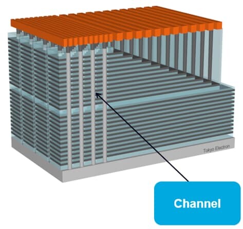
The innovative technology not only enables a 10-µm-deep etch with a high aspect ratio in just 33 minutes, but also can reduce the global warming potential by 84% compared with previous technologies. The geometry of the etched structure is quite well-defined as shown in the figure 1. Potential innovations enabled by this technology will spur creation of 3D NAND flash memory with even larger capacity.


The innovative technology not only enables a 10-µm-deep etch with a high aspect ratio in just 33 minutes, but also can reduce the global warming potential by 84% compared with previous technologies. The geometry of the etched structure is quite well-defined as shown in the figure 1. Potential innovations enabled by this technology will spur creation of 3D NAND flash memory with even larger capacity.