News Posts matching #TSMC N3

Return to Keyword Browsing

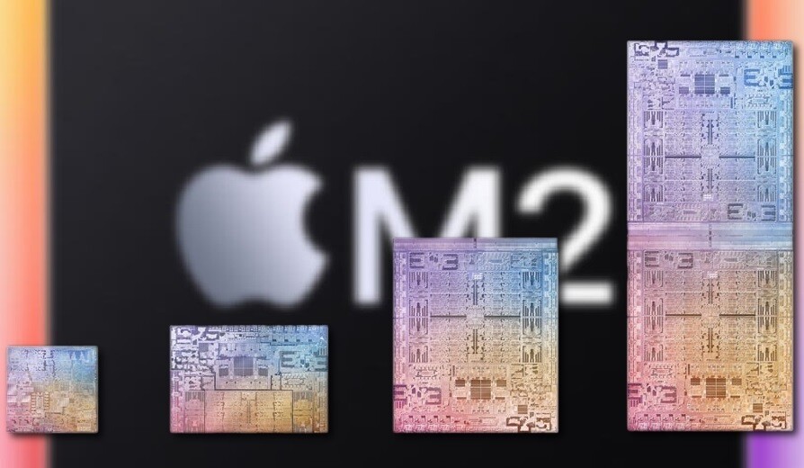
Apple M3 Ultra Chip Could be a Monolithic Design Without UltraFusion Interconnect

As we witness Apple's generational updates of the M series of chips, the highly anticipated SKU of the 3rd generation of Apple M series yet-to-be-announced top-of-the-line M3 Ultra chip is growing speculations from industry insiders. The latest round of reports suggests that the M3 Ultra might step away from its predecessor's design, potentially adopting a monolithic architecture without the UltraFusion interconnect technology. In the past, Apple has relied on a dual-chip design for its Ultra variants, using the UltraFusion interconnect to combine two M series Max chips. For example, the second generation M Ultra chip, M2 Ultra, boasts 134 billion transistors across two 510 mm² chips. However, die-shots of the M3 Max have sparked discussions about the absence of dedicated chip space for the UltraFusion interconnect.

While the absence of visible interconnect space on early die-shots is not conclusive evidence, as seen with the M1 Max not having visible UltraFusion interconnect and still being a part of M1 Ultra with UltraFusion, industry has led the speculation that the M3 Ultra may indeed feature a monolithic design. Considering that the M3 Max has 92 billion transistors and is estimated to have a die size between 600 and 700 mm², going Ultra with these chips may be pushing the manufacturing limit. Considering the maximum die size limit of 848 mm² for the TSMC N3B process used by Apple, there may not be sufficient space for a dual-chip M3 Ultra design. The potential shift to a monolithic design for the M3 Ultra raises questions about how Apple will scale the chip's performance without the UltraFusion interconnect. Competing solutions, such as NVIDIA's Blackwell GPU, use a high-bandwidth C2C interface to connect two 104 billion transistor chips, achieving a bandwidth of 10 TB/s. In comparison, the M2 Ultra's UltraFusion interconnect provided a bandwidth of 2.5 TB/s.

Intel, Marvell, and Synopsys to Showcase Next-Gen Memory PHY IP Capable of 224 Gbps on 3nm-class FinFET Nodes

The sneak peeks from the upcoming IEEE Solid State Circuit Conference continues, as the agenda items unveil interesting tech that will be either unveiled or demonstrated there. Intel, Synopsys, and Marvell, are leading providers of DRAM physical layer interface (PHY) IP. Various processor, GPU, and SoC manufacturers license PHY and memory controller IP from these companies, to integrate with their designs. All three companies are ready with over 200 Gbps around the 2.69 to 3 petajoule per bit range. This energy cost is as important as the data-rate on offer; as it showcases the viability of the PHY for a specific application (for example, a smartphone SoC has to conduct its memory sub-system at a vastly more constrained energy budget compared to an HPC processor).

Intel is the first in the pack to showcase a 224 Gbps sub-picojoule/bit PHY transmitter that supports PAM4 and PAM6 signaling, and is designed for 3 nm-class FinFET foundry nodes. If you recall, Intel 3 will be the company's final FinFET node before it transitions to nanosheets with the Intel 20A node. At the physical layer, all digital memory signal is analogue, and Intel's IP focuses on the DAC aspect of the PHY. Next up, is a somewhat similar transceiver IP by Synopsys. This too claims 224 Gbps speeds at 3 pJ/b, but at a 40 dB insertion loss; and is designed for 3 nm class FinFET nodes such as the TSMC N3 family and Intel 3. Samsung's 3 nm node uses the incompatible GAAFET technology for its 3 nm EUV node. Lastly, there's Marvell, with a 212 Gb/s DSP-based transceiver for optical direct-detect applications on the 5 nm FinFET nodes, which is relevant for high speed network switching fabrics.

Intel Lunar Lake-MX SoC with On-Package LPDDR5X Memory Detailed

With the reality of high performance Arm processors from Apple and Qualcomm threatening Intel's market share in the client computing space, Intel is working on learner more PCB-efficient client SoCs that can take the fight to them, while holding onto the foundations of x86. The first such form-factor of processors are dubbed -MX. These are essentially -U segment processors with memory on package, to minimize PCB footprint. Intel has fully integrated the PCH into the processor chip with "Meteor Lake," with PCH functions scattered across the SoC and I/O tiles of the processor. An SoC package with dimensions similar to those of -UP4 packages meant for ultrabooks, can now cram main memory, so the PCBs of next-generation notebooks can be further compacted.

Intel had recently shown Meteor Lake-MX packages to the press as a packaging technology demonstration in its Arizona facility. It's unclear whether this could release as actual products, but in a leaked company presentation, confirmed that its first commercial outing will be with Lunar Lake-MX. The current "Alder Lake-UP4" package measures 19 mm x 28.5 mm, and is a classic multi-chip module that combines a monolithic "Alder Lake" SoC die with a PCH die. The "Meteor Lake-UP4" package measures 19 mm x 23 mm, and is a chiplet-based processor, with a Foveros base tile that holds the Compute (CPU cores), Graphics (iGPU), SoC and I/O (platform core-logic) tiles. The "Lunar Lake-MX" package is slightly larger than its -UP4 predecessors, measuring 27 mm x 27.5 mm, but completely frees up space on the PCB for memory.

Apple Unveils New M3, M3 Pro, and M3 Max Processors on TSMC 3nm

Apple today announced M3, M3 Pro, and M3 Max, three chips featuring groundbreaking technologies that deliver dramatically increased performance and unleash new capabilities for Mac. These are the first personal computer chips built using the industry-leading 3-nanometer process technology, allowing more transistors to be packed into a smaller space and improving speed and efficiency. Together, M3, M3 Pro, and M3 Max show how far Apple silicon for the Mac has come since the debut of the M1 family of chips.

The M3 family of chips features a next-generation GPU that represents the biggest leap forward in graphics architecture ever for Apple silicon. The GPU is faster and more efficient, and introduces a new technology called Dynamic Caching, while bringing new rendering features like hardware-accelerated ray tracing and mesh shading to Mac for the first time. Rendering speeds are now up to 2.5x faster than on the M1 family of chips. The CPU performance cores and efficiency cores are 30 percent and 50 percent faster than those in M1, respectively, and the Neural Engine is 60 percent faster than the Neural Engine in the M1 family of chips. And, a new media engine now includes support for AV1 decode, providing more efficient and high-quality video experiences from streaming services. The M3 family of chips continues the tremendous pace of innovation in Apple silicon, and brings massive enhancements and new features to the new MacBook Pro and iMac.

Synopsys and TSMC Streamline Multi-Die System Complexity with Unified Exploration-to-Signoff Platform and Proven UCIe IP on TSMC N3E Process

Synopsys, Inc. today announced it is extending its collaboration with TSMC to advance multi-die system designs with a comprehensive solution supporting the latest 3Dblox 2.0 standard and TSMC's 3DFabric technologies. The Synopsys Multi-Die System solution includes 3DIC Compiler, a unified exploration-to-signoff platform that delivers the highest levels of design efficiency for capacity and performance. In addition, Synopsys has achieved first-pass silicon success of its Universal Chiplet Interconnect Express (UCIe) IP on TSMC's leading N3E process for seamless die-to-die connectivity.

"TSMC has been working closely with Synopsys to deliver differentiated solutions that address designers' most complex challenges from early architecture to manufacturing," said Dan Kochpatcharin, head of the Design Infrastructure Management Division at TSMC. "Our long history of collaboration with Synopsys benefits our mutual customers with optimized solutions for performance and power efficiency to help them address multi-die system design requirements for high-performance computing, data center, and automotive applications."

Synopsys, TSMC and Ansys Strengthen Ecosystem Collaboration to Advance Multi-Die Systems

Accelerating the integration of heterogeneous dies to enable the next level of system scalability and functionality, Synopsys, Inc. (Nasdaq: SNPS) has strengthened its collaboration with TSMC and Ansys for multi-die system design and manufacturing. Synopsys provides the industry's most comprehensive EDA and IP solutions for multi-die systems on TSMC's advanced 7 nm, 5 nm and 3 nm process technologies with support for TSMC 3DFabric technologies and 3Dblox standard. The integration of Synopsys implementation and signoff solutions and Ansys multi-physics analysis technology on TSMC processes allows designers to tackle the biggest challenges of multi-die systems, from early exploration to architecture design with signoff power, signal and thermal integrity analysis.

"Multi-die systems provide a way forward to achieve reduced power and area and higher performance, opening the door to a new era of innovation at the system-level," said Dan Kochpatcharin, head of Design Infrastructure Management Division at TSMC. "Our long-standing collaboration with Open Innovation Platform (OIP) ecosystem partners like Synopsys and Ansys gives mutual customers a faster path to multi-die system success through a full spectrum of best-in-class EDA and IP solutions optimized for our most advanced technologies."

Reports Suggest MacBook Air Models Rocking M3 Chipset Incoming, But Delayed Beyond WWDC 2023

Conflicting reports are flying around about Apple's next generation MacBook Air lineup, mostly surrounding suggestions of a firm release date or debut reveal at WWDC 2023. 9to5Mac claims that its insider sources have pointed to a new range of M3 chipset powered MacBook Air extra thin laptops offered up in two different screen sizes: 13-inch and 15-inch. An insider claimed last month that Apple's upcoming laptop lineup was in an advanced stage of production, and was far along enough to warrant an "imminent" launch window. A Taiwanese publication has presented new evidence this week, and it posits that Apple could drop M3 chipset-based laptops from announcement presentations organized for this year's Worldwide Developers Conference, which is set to take place from June 5 to 9.

According to the financial section of Taiwan's UDN news site, Apple's key decision makers could be in favor of fielding laptops based on its current generation M2 SoC, instead of an entry-level M3-based range, due to delays and changes in priority for the N3B node at TSMC foundries. This is seen as an odd move given reports from earlier this month of Apple requesting a reduction in factory output for its M2 chips, following a slump in demand. Apple could be changing its strategy with regards to the alleged surplus of M2 silicon - the article theorizes that the company will spend more time fitting the older generation chipsets into a new range of laptops and desktop computers. An M3-based product line could be delayed into late 2023, and it is alleged that TSMC has been instructed to concentrate mostly on manufacturing Apple's Bionix A17 mobile chipset via the cutting edge 3 nm FinFet technology process (N3B) - earmarked to debut on the iPhone 15 Pro in autumn 2023.

Snapdragon 8 Gen 3 GPU Could be 50% More Powerful Than Current Gen Adreno 740

An online tipster, posting on the Chinese blog site Weibo, has let slip that Qualcomm's upcoming Snapdragon 8 Gen 3 mobile chipset is touted to pack some hefty graphical capabilities. The suggested Adreno "750" smartphone and tablet GPU is touted to offer a 50% increase over the present generation Adreno 740 - as featured on the recently released and cutting-edge Snapdragon 8 Gen 2 chipset. The current generation top-of-the-range Snapdragon is no slouch when it comes to graphics benchmarks, where it outperforms Apple's prime contender - the Bionic A16 SoC.

The Snapdragon 8 Gen 3 SoC is expected to launch in the last quarter of 2023, but details of the flagship devices that it will power are non-existent at the time of writing. The tipster suggests that Qualcomm has decided to remain on TSMC's 4 nm process for its next generation mobile chipset - perhaps an all too safe decision when you consider that Apple has upped the stakes with the approach of its Bionic A17 SoC. It has been reported that the Cupertino, California-based company has chosen to fabricate via TSMC's 3 nm process, although the Taiwanese foundry is said to be struggling with its N3 production line. The engineers at Qualcomm's San Diego headquarters are alleged to be experimenting with increased clock speeds running on the next gen Adreno GPU - as high as 1.0 GHz - in order to eke out as much performance as possible, in anticipation of besting the Bionic A17 in graphics benchmarks. The tipster theorizes that Qualcomm will still have a hard time matching Apple in terms of pure CPU throughput, so the consolation prize will lie with a superior GPU getting rigged onto the Snapdragon 8 Gen 3.

Apple A17 Bionic SoC Performance Targets Could be Lowered

Apple's engineering team is rumored to be adjusting performance targets set for its next generation mobile SoC - the A17 Bionic - due to issues at the TSMC foundry. The cutting edge 3 nm process is proving difficult to handle, according to industry tipsters on Twitter. The leaks point to the A17 Bionic's overall performance goals being lowered by 20%, mainly due to the TSMC N3B node not meeting production targets. The factory is apparently lowering its yield and execution targets due to ongoing problems with FinFET limitations.

The leakers have recently revealed more up-to-date A17 Bionic's Geekbench 6 scores, with single thread performance at 3019, and multi-thread at 7860. Various publications have been hyping the mobile SoC's single thread performance as matching that of desktop CPUs from Intel and AMD, more specifically 13th-gen Core i7 and 'high-end' Ryzen models. Naturally the A17 Bionic cannot compete with these CPUs in terms of multi-thread performance.

Intel Defers 3 nm Wafer Orders with TSMC, Pushes "Arrow Lake" Rollout to 2025?

Intel has reportedly deferred its orders for 3 nm wafers with TSMC, sources in PC makers tell Taiwan-based industry observer DigiTimes. Built on the TSMC N3 node, the wafers were supposed to power the Graphics tiles (containing the iGPU), of the upcoming "Arrow Lake" processors, which were originally on course for a 2024 release. The DigiTimes report detailing this development says that Intel's 3 nm wafer orders have been deferred to Q4-2024, which would realistically mean a 2025 launch for whatever product was designed to use 3 nm tiles. Advance orders for next-gen wafers by high-volume clients such as Intel, are usually placed several quarters in advance, so the foundry could suitably scale up its capacity.

Alphawave IP Achieves Its First Testchip Tapeout for TSMC N3E Process

Alphawave IP (LSE: AWE), a global leader in high-speed connectivity for the world's technology infrastructure, today announced the successful tapeout of its ZeusCORE100 1-112 Gbps NRZ/PAM4 Serialiser-Deserialiser ("SerDes"), Alphawave's first testchip on TSMC's most advanced N3E process. Alphawave IP will be exhibiting this new product alongside its complete portfolio of high-performance IP, chiplet, and custom silicon solutions at the TSMC OIP Forum on October 26 in Santa Clara, CA as the Platinum sponsor.

ZeusCORE100 is Alphawave's most advanced multi-standard-SerDes, supporting extra-long channels over 45dB and the most requested standards such as 800G Ethernet, OIF 112G-CEI, PCIe GEN6, and CXL 3.0. Attendees will be able to visit the Alphawave booth and meet the company's technology experts including members of the recently acquired OpenFive team. OpenFive is a longstanding partner of TSMC through the OIP Value Chain Aggregator (VCA) program. OpenFive is one of a select few companies with an idea-to-silicon methodology in TSMC's latest technologies, and advanced packaging capabilities, enabling access to the most advanced foundry solution available with the best Power-Performance-Area (PPA). With Alphawave's industry-leading IP portfolio and the addition of OpenFive's capabilities, designers can create systems on a chip (SoCs) that pack more compute power into smaller form factors for networking, AI, storage, and high-performance computing (HPC) applications.

Intel 14th Gen "Meteor Lake" APUs Reportedly Feature Ray Tracing, May Lack XeSS

Intel's future Meteor Lake APUs seem to be playing catch-up to AMD's integrated graphics in more ways than one. Twitter user Coelacanth's Dream has dug up information that indicates Intel's commitment to bring ray tracing support to even its IGP (Integrated Graphics Processing) tiles. According to bits and pieces from Intel Graphics Compiler (IGC) code patches, it seems to be confirmed that ray tracing support is indeed coming to the TSMC-made, 3 nm GPU tiles in Meteor Lake. The kicker here is the presence of flags that detect whether the iGPU is of the "iGFX_meteorlake" type - if so, IGC sets ray tracing support to enabled.

Puzzlingly, Intel's upscaling technology, Xe SuperSampling (XeSS) could be out of the picture - at least for now. It seems that IGC patches for the upcoming APU family still don't allow for DPAS (Dot Product Accumulate Systolic) instructions - instructions that rely on XMX (Intel Xe Matrix Extensions), the AI engines responsible for executing 128 FP16/BF16, 256 INT8, or 512 INT4/INT2 operations per clock. These low-precision operations are the soul of algorithmic supersampling technologies such as XeSS.
Return to Keyword Browsing
Apr 29th, 2024 15:37 EDT change timezone

New Forum Posts

Popular Reviews

Controversial News Posts