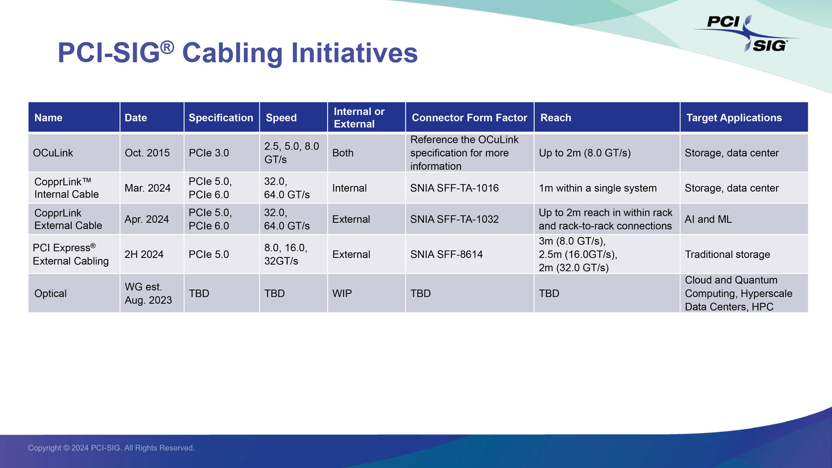
News Posts matching #Technology

Return to Keyword Browsing

IBM Power11 Raises the Bar for Enterprise IT

Today, IBM revealed IBM Power11, the next generation of IBM Power servers. Redesigned with innovations across its processor, hardware architecture, and virtualization software stack, Power11 is designed to deliver the availability, resiliency, performance, and scalability enterprises demand, for seamless hybrid deployment on-premises or in IBM Cloud.

Organizations across industries have long run their most mission-critical, data-intensive workloads on IBM Power, most notably those within the banking, healthcare, retail, and government spaces. Now, enterprises face an onslaught of new technologies and solutions as they transition into the age of AI. IDC found that one billion new logical applications are expected by 2028, and the proliferation of these systems poses new complexities for companies. IBM built Power11 to deliver simplified, always-on operations with hybrid cloud flexibility for enterprises to maintain competitiveness in the AI era.

LG Innotek CEO Moon Hyuksoo: "Our Next-gen Substrate Technology Will Change the Industry Paradigm"

LG Innotek is continuing its quest to become the world's top company in the field of technology components, with its latest milestone being the successful development of an innovative semiconductor substrate technology. LG Innotek (CEO Moon Hyuksoo) announced on July 3rd that it successfully developed and started mass-producing the world's first copper post (Cu-Post) technology, which is applicable high-value-added semiconductor substrates for mobile devices.

With major manufacturers racing to make smartphones ever thinner, ways to minimize the size of smartphone components have become increasingly sought after. Demand is soaring for mobile device semiconductor substrates that provide maximum performance in a minimal size, such as the RF-SiP (Radio Frequency-System in Package) substrate.

LG Display Begins Mass Production of Ultimate Gaming OLED Panel with 4th-Generation OLED Technology

LG Display, the world's leading innovator of display technologies, announced today that it has successfully begun mass production of the world's top OLED monitor panel, incorporating its latest proprietary technology as the company accelerates its push into the premium monitor panel market. The 27-inch OLED monitor panel achieves a peak brightness of 1,500 nits thanks to the application of the company's core fourth-generation OLED technology, Primary RGB Tandem.

In addition, LG Display has successfully developed a 540 Hz OLED monitor panel - surpassing the highest refresh rate currently available - and plans to unveil it soon. As a result, LG Display is leading the world's OLED technology across the "triple crown" of key elements that determine gaming monitor picture quality - brightness, refresh rate, and response time.

DDR4 Module Prices Overtake DDR5 for the First Time

Usually for newer technology rollout, prices are significantly higher compared to the last-gen. However, with DRAM, the story is the opposite. For the first time since the launch of DDR5, buyers are paying more for DDR4 memory modules than for the newer standard. A combination of tariff uncertainty and rapidly depleting DDR4 inventories is the main driver behind this. TrendForce data show that some high-demand DDR4 kits rose by as much as 40% in just one week, while DRAMeXchange reports that the average spot price for a 16 Gb (1Gx16) DDR4 module at 3,200 MT/s from Samsung and SK Hynix climbed to $12.50, with peak offers hitting $24. By contrast, dual-8 Gb DDR5 kits running between 4,800 MT/s and 5,600 MT/s remain near $6 on average, rarely exceeding $9. This unexpected surge follows Micron's announcement that it will wind down DDR4 production by year's end, accelerating the depletion of existing stocks over the next six to nine months.

Samsung also announced plans earlier this spring to retire its DDR4 lines and shift its focus to DDR5 and high-bandwidth memory, while China's CXMT confirmed it will scale back its DDR4 output despite recently reaching peak production levels. Taiwan's Nanya Technology is among the biggest beneficiaries of this topsy-turvy market. In the first quarter, the company held a DDR4 inventory valued at approximately NT$37.6 billion ($1.2 billion). Nanya even paused public price quoting to manage sales at these elevated levels. Many in the tech industry worry that renewed US-China trade tensions could spark another wave of panic buying. If additional tariffs target China's remaining DDR4 supply, module costs could climb to more than three times the price of DDR5, extending this rare pricing inversion well into the next quarter.

IBM and RIKEN Unveil First IBM Quantum System Two Outside of the U.S.

IBM and RIKEN, a national research laboratory in Japan, today unveiled the first IBM Quantum System Two ever to be deployed outside of the United States and beyond an IBM Quantum Data Center. The availability of this system also marks a milestone as the first quantum computer to be co-located with RIKEN's supercomputer Fugaku—one of the most powerful classical systems on Earth. This effort is supported by the New Energy and Industrial Technology Development Organization (NEDO), an organization under the jurisdiction of Japan's Ministry of Economy, Trade and Industry (METI)'s "Development of Integrated Utilization Technology for Quantum and Supercomputers" as part of the "Project for Research and Development of Enhanced Infrastructures for Post 5G Information and Communications Systems."

IBM Quantum System Two at RIKEN is powered by IBM's 156-qubit IBM Quantum Heron, the company's best performing quantum processor to-date. IBM Heron's quality as measured by the two-qubit error rate, across a 100-qubit layered circuit, is 3x10⁻³ (with the best two-qubit error being 1x10⁻³)—which is 10 times better than the previous generation 127-qubit IBM Quantum Eagle. IBM Heron's speed, as measured by the CLOPS (circuit layer operations per second) metric is 250,000, which reflects another 10x improvement in the past year, over IBM Eagle.

Samsung Reportedly Achieves 70% Yields for Its 1c DRAM Technology

Samsung has achieved better production results for its advanced memory technology, according to Sedaily, as cited by TrendForce. The company's sixth-generation 10 nm DRAM, called 1c DRAM, now shows yield rates of 50-70% in testing. This represents a significant improvement from last year's results, which were below 30%. Samsung takes a different path from its rivals, while SK Hynix and Micron stick with 1b DRAM technology for HBM4 products, Samsung opts to create the newer 1c DRAM. This choice comes with more risk; however, it might bring bigger rewards, as the improved production rates enable Samsung to expand its manufacturing operations. The company plans to increase 1c DRAM production at its Hwaseong and Pyeongtaek facilities with expansion activities expected to begin before the end of this year.

These developments also support Samsung's HBM4 production schedule since the company aims to begin mass production of HBM4 products later this year. Yet, experts in the field point out that the product is still in its early stages and needs ongoing monitoring. Samsung planned to begin mass-producing sixth-gen 10 nm DRAM by late 2024. Instead, the company chose to remake the chip's design. This decision caused delays of more than one year however it was made to achieve better performance and yields. The new DRAM products will be manufactured at Samsung's Pyeongtaek Line 4 facility as these chips will serve both mobile and server applications. Separately, HBM4-related production will take place at Pyeongtaek Line 3.

LG Display to Invest Over US$900M Into OLED Technology Differentation

LG Display, the world's leading innovator of display technologies, announced today that it plans to make an investment in new OLED technologies at the trillion-KRW level to enhance its technological competitiveness and growth foundation. The company's board met on June 17 and approved an investment of KRW 1.26 trillion in new OLED technologies to secure a leading position in the display market.

It will focus on infrastructure development, including facilities for applying new OLED technologies. The investment period has been set for approximately two years, from June 17, 2025, to June 30, 2027. This investment is part of LG Display's mid- to long-term capital expenditure (CAPEX) plan, and efforts to improve the company's financial structure will continue independently of it.

Micron and Trump Administration Announce Expanded U.S. Investments in Leading-Edge DRAM Manufacturing and R&D

Micron Technology, Inc. (Nasdaq: MU) and the Trump Administration today announced Micron's plans to expand its U.S. investments to approximately $150 billion in domestic memory manufacturing and $50 billion in R&D, creating an estimated 90,000 direct and indirect jobs. As part of today's announcement, Micron plans to invest an additional $30 billion beyond prior plans which includes building a second leading-edge memory fab in Boise, Idaho; expanding and modernizing its existing manufacturing facility in Manassas, Virginia; and bringing advanced packaging capabilities to the U.S. to enable long-term growth in High Bandwidth Memory (HBM), which is essential to the AI market. Additionally, Micron is announcing a planned $50 billion domestic R&D investment, reaffirming its long-term position as the global memory technology leader. As previously announced, Micron's investment includes its ongoing plans for a megafab in New York.

Micron's approximately $200 billion broader U.S. expansion vision includes two leading-edge high-volume fabs in Idaho, up to four leading-edge high-volume fabs in New York, the expansion and modernization of its existing manufacturing fab in Virginia, advanced HBM packaging capabilities and R&D to drive American innovation and technology leadership. These investments are designed to allow Micron to meet expected market demand, maintain share and support Micron's goal of producing 40% of its DRAM in the U.S. The co-location of these two Idaho fabs with Micron's Idaho R&D operations will drive economies of scale and faster time to market for leading-edge products, including HBM.

Alphawave Semi Tapes Out New UCIe IP on TSMC 2nm Supporting 36G Die-to-Die Data Rates

Alphawave Semi, a global leader in high-speed connectivity and compute silicon for the world's technology infrastructure, announced the successful tape out of one of the industry's first UCIe IP subsystem on TSMC's N2 process, supporting 36G die-to-die data rates. The solution is fully integrated with TSMC's Chip-on-Wafer-on-Substrate (CoWoS ) advanced packaging technology, unlocking breakthrough bandwidth density and scalability for next-generation chiplet architectures.

This milestone builds on the recent release of the Alphawave Semi AI Platform, proving readiness to support the future of disaggregated SoCs and scale-up infrastructure for hyperscale AI and HPC workloads. With this tape-out, Alphawave Semi becomes one of the industry's first to enable UCIe connectivity on 2 nm nanosheet technology, marking a major step forward for the open chiplet ecosystem.

Micron Ships World's First 1γ (1-Gamma)-Based LPDDR5X

Micron Technology, Inc. (Nasdaq: MU), announced today that it is shipping qualification samples of the world's first 1γ (1-gamma) node-based low-power double data rate 5X (LPDDR5X) memory, designed to accelerate AI applications on flagship smartphones. Delivering the industry's fastest LPDDR5X speed grade of 10.7 gigabits per second (Gbps), combined with up to a 20% power savings, Micron LPDDR5X transforms smartphones with faster, smoother mobile experiences and longer battery life - even when executing data-intensive workloads such as AI-powered translation or image generation.

To meet the industry's increasing demand for compact solutions for next-generation smartphone designs, Micron's engineers have shrunk the LPDDR5X package size to offer the industry's thinnest package of 0.61 millimeters, making it 6% thinner compared to competitive offerings, and representing a 14% height reduction from the previous generation. The small form factor unlocks more possibilities for smartphone manufacturers to design ultrathin or foldable smartphones.

BenQ Launches ScreenBar Halo 2 Monitor Light

BenQ, the pioneer of monitor lighting solutions, today launched the ScreenBar Halo 2, its next-generation flagship monitor light engineered to deliver optimal eye comfort for professionals working in dim environments. Developed over four years, the ScreenBar Halo 2 enhances workspace lighting through a powerful dual-light design that provides full front and rear illumination.

Building on the success of its predecessor, the ScreenBar Halo 2 introduces a Tri-zone Backlight Design that expands coverage by 423%, reducing contrast between the monitor and its surroundings to ease visual fatigue. The front light features BenQ's ASYM-Light, an asymmetrical optical design with an 18-degree cut-off angle that eliminates screen glare and prevents direct light from reaching the eyes.

Intel Details EMIB-T Advanced Packaging for HBM4 and UCIe

This week at the Electronic Components Technology Conference (ECTC), Intel introduced EMIB-T, an important upgrade to its embedded multi-die interconnect bridge packaging. First showcased at the Intel Foundry Direct Connect 2025 event, EMIB-T incorporates through-silicon vias (TSVs) and high-power metal-insulator-metal capacitors into the existing EMIB structure. According to Dr. Rahul Manepalli, Intel Fellow and vice president of Substrate Packaging Development, these changes allow a more reliable power supply and stronger communication between separate chiplets. Conventional EMIB designs have struggled with voltage drops because of their cantilevered power delivery paths. In contrast, EMIB-T routes power directly through TSVs from the package substrate to each chiplet connection. The integrated capacitors compensate for fast voltage fluctuations and preserve signal integrity.

This improvement will be critical for next-generation memory, such as HBM4 and HBM4e, where data rates of 32 Gb/s per pin or more are expected over a UCIe interface. Intel has confirmed that the first EMIB-T packages will match the current energy efficiency of around 0.25 picojoules per bit while offering higher interconnect density. The company plans to reduce the bump pitch below today's standard of 45 micrometers. Beginning in 2026, Intel intends to produce EMIB-based packages measuring 120 by 120 millimeters, roughly eight times the size of a single reticle. These large substrates could integrate up to twelve stacks of high-bandwidth memory alongside multiple compute chiplets, all connected by more than twenty EMIB bridges. Looking further ahead, Intel expects to push package dimensions to 120 by 180 millimeters by 2028. Such designs could accommodate more than 24 memory stacks, eight compute chiplets, and 38 or more EMIB bridges. These developments closely mirror similar plans announced by TSMC for its CoWoS technology. In addition to EMIB-T, Intel also presented a redesigned heat spreader that reduces voids in the thermal interface material by approximately 25%, as well as a new thermal-compression bonding process that minimizes warping in large package substrates.

xMEMS Extends µCooling Fan-on-a-Chip Technology to Data Centers SSDs

xMEMS Labs, Inc., the pioneer of monolithic MEMS-based solutions, today announced the expansion of its revolutionary µCooling fan-on-a-chip platform into AI data centers, bringing the industry's first in-module active thermal management solution to high-performance optical transceivers. Originally developed for compact mobile devices, xMEMS µCooling now provides targeted, hyper-localized active cooling for dense, thermally-challenged environments inside 400G, 800G, and 1.6T optical transceivers—a critical yet underserved category in next-gen AI infrastructure.

Unlike conventional cooling approaches that target high-power (kilowatt) processors and GPUs, µCooling focuses on smaller, thermally stressed components that large-scale cooling systems can't reach, such as optical transceiver DSPs, that operate at 18 W TDP or higher. These components introduce thermal challenges and increasingly limit transceiver performance and reliability as data rates scale.

THX Announces THX Spatial Audio+, New Immersive Audio Platform for Laptops, Headphones and Soundbars

THX, Ltd., a world-class high-fidelity audio and video tuning, certification, and technology company, and producer of the iconic THX Deep Note Trailers, has announced today the expansion of its THX Spatial Audio technology. Innovating for enjoyment of gaming, movies and music while listening on consumer electronics and mobile devices such as laptops, headphones, earbuds and soundbars, THX today announced a feature-rich new immersive audio architecture, THX Spatial Audio+.

To ensure that gamers and audio- and videophiles alike can enjoy the pinpoint audio accuracy and true-to-life realism of immersive entertainment like never before comes THX Spatial Audio+. THX Spatial Audio+ improves the core spatial experience with an enhanced and flexible architecture designed to support continued innovation, including such unique features as adding height channels to the immersion and camera-based AI head tracking, depending upon the demands of the device.

Audioscenic Implements BeClear Technology to Demonstrate World's First Hi-D Soundbar Design with Gaming Voice Chat

Audioscenic, the UK-based audio technology innovator, announces a technology collaboration with Philips and semiconductor solutions leader NXP Semiconductors, to demonstrate the world's first reference design for gaming soundbars. This breakthrough combines Audioscenic Amphi Hi-D spatial audio featuring AI position sensing with Acoustic Echo Cancellation (AEC) from Philips BeClear. Powered by the NXP i.MX 8M Mini applications processor, this technology enables soundbar manufacturers to deliver fully immersive, location-accurate game audio simultaneously with crystal-clear voice chat—a combination previously unachievable in gaming soundbars. Product designers, product managers, and engineers can experience the reference design in person at Computex Taipei 2025.

Gamers have long faced a trade-off: enjoy rich, immersive sound through speakers or have clear voice communication with teammates through headsets. While headsets have dominated hardcore gaming, many players prefer speaker systems like soundbars for extended comfort without headset fatigue, and a more natural "room-filling" audio experience versus the inside-your-head sound of headsets.

Infineon Announces Collaboration with NVIDIA on Power Delivery Chips for Future Server Racks

Infineon Technologies AG is revolutionizing the power delivery architecture required for future AI data centers. In collaboration with NVIDIA, Infineon is developing the next generation of power systems based on a new architecture with central power generation of 800 V high-voltage direct current (HVDC). The new system architecture significantly increases energy-efficient power distribution across the data center and allows power conversion directly at the AI chip (Graphic Processing Unit, GPU) within the server board. Infineon's expertise in power conversion solutions from grid to core based on all relevant semiconductor materials silicon (Si), silicon carbide (SiC) and gallium nitride (GaN) is accelerating the roadmap to a full scale HVDC architecture.

This revolutionary step paves the way for the implementation of advanced power delivery architectures in accelerated computing data centers and will further enhance reliability and efficiency. As AI data centers already are going beyond 100,000 individual GPUs, the need for more efficient power delivery is becoming increasingly important. AI data centers will require power outputs of one megawatt (MW) and more per IT rack before the end of the decade. Therefore, the HVDC architecture coupled with high-density multiphase solutions will set a new standard for the industry, driving the development of high-quality components and power distribution systems.

Samsung Display Presents Its Most Advanced OLED Technology at Computex 2025

Samsung Display is participating in COMPUTEX TAIPEI 2025, Asia's largest IT trade show, for the first time, showcasing its cutting-edge OLED display technologies. The company announced today that it will exhibit at COMPUTEX TAIPEI 2025, taking place May 20 to 23 at the Taipei Nangang Exhibition Center Hall 2, it will host a private exhibition for clients, unveiling its latest IT OLED portfolio for applications like laptops, tablets, monitors and other IT devices.

Samsung Display is set to unveil UT One for the first time alongside a range of low-power solutions optimized for IT devices such as laptops and tablets. The company will also showcase QD-OLED prototypes along with an ultra-high resolution and ultra-high refresh rate that will change the premium monitor market. In addition, wheeled dual-arm robots Rainbow Robotics, a company that specializes in robotic platforms, will perform a welcome show to demonstrate the slimness and light weight characteristics of Samsung OLED, set to leave a lasting impression on clients visiting our booth.

Microchip Brings Hardware Quantum Resistance to Embedded Controllers

Driven by advancements in cryptographic research and the need for stronger security measures, the National Security Agency (NSA) introduced the Commercial National Security Algorithm Suite 2.0 (CNSA 2.0) to establish a set of quantum-resistant cryptographic standards. The NSA is now urging data center and computing markets to become post-quantum ready within the next two years. To help system architects meet evolving security demands, Microchip Technology has developed its MEC175xB embedded controllers with embedded immutable post-quantum cryptography support.

As a standalone controller, the MEC175xB family employs a modular approach for developers to efficiently adopt post-quantum cryptography, helping ensure long-term data protection without compromising existing functionality. These low-power controllers are designed with National Institute of Standards and Technology (NIST) approved post-quantum cryptographic algorithms, configurable secure boot solutions and an advanced Enhanced Serial Peripheral Interface (eSPI).

Samsung Display Unveils Advanced R&D Achievements at Display Week 2025

Samsung Display announced on May 13 that it will take part in Display Week 2025, held from May 13 to 15 at the McEnery Convention Center in San Jose, California. The event, hosted by the Society for Information Display (SID), brings together display companies and experts from around the world to share cutting-edge technologies and R&D achievements.

Samsung Display is set to unveil a range of next-generation display technologies, including the industry's first non-cadmium 400-nit EL-QD and a 5,000 pixels-per-inch (PPI) RGB OLED on Silicon (OLEDoS) at Display Week 2025, reinforcing its leadership in cutting-edge panel technology. The company will also highlight its leadership in OLED innovation through a range of future-oriented technologies, including organic photodiodes (OPD), advanced sensors capable of measuring biometric data such as heart rate and blood pressure directly from light generated by a panel touched by a patient, and a high-resolution microdisplay that delivers 5,000 PPI in a compact 1.4-inch form factor.

Intel Sunsets "Deep Link" Technology Suite, Ending Future Development and Support

Intel is officially stepping back from its Deep Link suite of technologies. The confirmation came through a company representative on GitHub, confirming that active development has ceased. This follows a period when Intel quietly stopped highlighting Deep Link in newer offerings, such as its "Battlemage" GPUs. While the features might still work for those currently using Deep Link, don't expect any future updates or official assistance from Intel's support channels. If you cast your mind back to late 2020, you might recall Intel launching Deep Link. The core idea was to get Intel CPUs and their dedicated Arc GPUs working more effectively in tandem. To tap into this, you needed a specific setup: an 11th, 12th, or 13th Generation Intel CPU alongside an Arc Alchemist GPU. The package featured key tools: Dynamic Power Share for optimizing power between the CPU and GPU, Stream Assist to offload streaming to integrated graphics, Hyper Encode for faster video encoding, and Hyper Compute to accelerate AI tasks using OpenVINO.

These were designed to give a leg up to applications like OBS, DaVinci Resolve, and Handbrake. However, the writing may have been on the wall for Deep Link. Intel's "Meteor Lake" chips, which arrived in late 2023, weren't on the compatibility list, hinting that development had already wound down. Getting these features to perform reliably wasn't always straightforward, with users, like the one on GitHub who raised the initial question, reporting difficulties even with supported hardware. A user tried running Core Ultra 200S with Battlemage in OBS, facing issues not by the software, but by Intel's drivers. The general thinking is that Intel might have viewed Deep Link as a bit of a niche feature, possibly concluding that the continued effort and investment, especially with the need for validation with each software vendor, wasn't paying off. As for what's next, Intel hasn't announced a direct successor to these specific integrated features.

NEO Semiconductor Unveils Breakthrough 1T1C and 3T0C IGZO-Based 3D X-DRAM Technology

NEO Semiconductor, a leading developer of innovative technologies for 3D NAND flash memory and 3D DRAM, announced today the latest advancement in its groundbreaking 3D X-DRAM technology family—the industry-first 1T1C- and 3T0C-based 3D X-DRAM cell, a transformative solution designed to deliver unprecedented density, power efficiency, and scalability for the most demanding data applications.

Built on a 3D NAND-like architecture and with proof-of-concept test chips expected in 2026, the new 1T1C and 3T0C designs combine the performance of DRAM with the manufacturability of NAND, enabling cost-effective, high-yield production with densities up to 512 Gb—a 10x improvement over conventional DRAM.
"With the introduction of the 1T1C and 3T0C 3D X-DRAM, we are redefining what's possible in memory technology," said Andy Hsu, Founder & CEO of NEO Semiconductor. "This innovation pushes past the scaling limitations of today's DRAM and positions NEO as a frontrunner in next-generation memory."

Component Shortages Delay Taiwanese Electronics Firms' U.S. Expansion

Taiwan's electronics manufacturing services (EMS) providers are accelerating their North American production plans in response to tariff threats, but component shortages and capacity constraints at US chip plants could hamper the AI server market for years, according to industry sources.

"Since Trump's election, Taiwanese manufacturers have been strategically expanding their US presence," said Yen Chou, an analyst at DIGITIMES Research. "Most server manufacturers are concentrating in Texas, with Foxconn's FII already operating there and planning expansions."

Astera Labs Ramps Production of PCIe 6 Connectivity Portfolio

Astera Labs, Inc., a global leader in semiconductor-based connectivity solutions for AI and cloud infrastructure, today announced its purpose-built PCIe 6 connectivity portfolio is ramping production to fast-track deployments of modern AI platforms at scale. Now featuring gearbox connectivity solutions alongside fabric switches, retimers, and active cable modules, Astera Labs' expanding PCIe 6 portfolio provides a comprehensive connectivity platform to deliver unparalleled performance, utilization, and scalability for next-generation AI and general-compute systems. Along with Astera Labs' demonstrated PCIe 6 connectivity over optical media, the portfolio will provide even greater AI rack-scale distance optionality. The transition to PCIe 6 is fueled by the insatiable demand for higher compute, memory, networking, and storage data throughput, ensuring advanced AI accelerators and GPUs operate at peak efficiency.

Thad Omura, Chief Business Officer, said, "Our PCIe 6 solutions have successfully completed qualification with leading AI and cloud server customers, and we are ramping up to volume production in parallel with their next generation AI platform rollouts. By continuing to expand our industry-leading PCIe connectivity portfolio with additional innovative solutions that includes Scorpio Fabric Switches, Aries Retimers, Gearboxes, Smart Cable Modules, and PCIe over optics technology, we are providing our hyperscaler and data center partners all the necessary tools to accelerate the development and deployment of leading-edge AI platforms."

China Rumored to Acquire 12-High HBM3E Bonders Through Korean Companies

China is pushing forward with its HBM (High Bandwidth Memory) progress as part of its plan to be self-sufficient in the semiconductor industry. JCET Group, China's top semiconductor packaging firm, has bought advanced TC (thermal compression) bonders that are usually used for 12-high stacks of HBM3E chips, according to Money Today Korea (MTN). This state-of-the-art equipment comes from Korean companies where export rules are less strict. This lets China jump from its current HBM2 technology to more advanced memory solutions. However, even if China isn't yet going to produce HBM3E chips soon, having this equipment is useful to boost manufacturing yields even for lower-spec HBM products.

China's desire to make HBM chips at home is a reaction to U.S. rules and taxes meant to hold back its chip abilities. These steps haven't slowed progress; instead, they have made China more determined to stand on its own in chip-making. The AI chip design market hit $18.4 billion last year and is set to grow 28% each year until 2032. The plan aims to supply Chinese-made HBM chips to big tech firms like Huawei, Tencent, and DeepSeek. This helps China get around U.S. export limits while moving its chip industry up in value. Choi Jae-hyeok, Professor of Electrical and Information Engineering, Seoul National University says, "In China's case, it is government-led... In the case of DDR, they are making up to DDR4 and DDR5. China has always wanted to move from low-value-added products to high-value-added products. The next direction is HBM..."

LG Display First to Verify Commercialization-Level Performance of Blue Phosphorescent OLED Panels

LG Display, the world's leading innovator of display technologies, announced today that it has become the world's first company to successfully verify the commercialization-level performance of blue phosphorescent OLED panels on a mass production line. The achievement comes about eight months after the company partnered with UDC to develop blue phosphorescence, and is considered a significant step closer to realizing a "dream OLED" display.

In the display industry, "dream OLED" refers to an OLED panel that achieves phosphorescence for all three primary colors of light (red, green, and blue). OLED panel light emission methods are broadly categorized into fluorescence and phosphorescence. Fluorescence is a simpler process in which materials emit light immediately upon receiving electrical energy, but its luminous efficiency is only 25%. In contrast, phosphorescence briefly stores received electrical energy before emitting light. Although it is technically more complex, this method offers luminous efficiency of 100% and uses a quarter as much power as fluorescence.
Return to Keyword Browsing
Jul 8th, 2025 12:42 CDT change timezone

New Forum Posts

Popular Reviews

TPU on YouTube

Controversial News Posts