News Posts matching #Xperi

Return to Keyword Browsing

SK Hynix Details its Upcoming HBM3 Memory: 665 GB/s per Stack

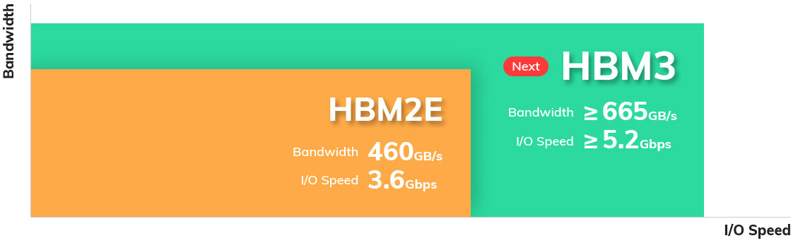
SK Hynix is at the forefront of developing the next generation of stacked high-bandwidth memory, the HBM3 standard. Succeeding the current HBM2e standard, HBM3 will power next-generation HPC and AI processors in high-density multi-chip modules. A Tom's Hardware report citing information from SK Hynix reveals two key details about the new standard. For starters, it could offer per-pin data-rates of 5.2 Gbps, a 44% increase over the 3.6 Gbps that HBM2e caps out at. This results in a per-stack bandwidth of 665 GB/s, compared to 480 GB/s for the HBM2e. A processor with four such stacks (over a 4096-bit wide bus), would hence enjoy 2.66 TB/s of memory bandwidth. It's likely that HBM3 stacks from SK Hynix could implement the DBI Ultra 2.5D/3D hybrid bonding interconnect technology licensed from Xperi Corp.

SK Hynix Licenses DBI Ultra 3D Interconnect Technology

Xperi Corporation today announced that it entered into a new patent and technology license agreement with SK hynix, one of the world's largest semiconductor manufacturers. The agreement includes access to Xperi's broad portfolio of semiconductor intellectual property (IP) and a technology transfer of Invensas DBI Ultra 3D interconnect technology focused on next-generation memory.

"We are delighted to announce the extension of our long-standing relationship with SK hynix, a world-renowned technology leader and manufacturer of memory solutions," said Craig Mitchell, President of Invensas, a wholly owned subsidiary of Xperi Corporation. "As the industry increasingly looks beyond conventional node scaling and turns toward hybrid bonding, Invensas stands as a pioneering leader that continues to deliver improved performance, power, and functionality, while also reducing the cost of semiconductors. We are proud to partner with SK hynix to further develop and commercialize our DBI Ultra technology and look forward to a wide range of memory solutions that leverage the benefits of this revolutionary technology platform."

NVIDIA Sued by Company Behind Big Samsung and Broadcom IP Dispute Wins

NVIDIA has been patent-trolled sued over patent-infringement by Xperi, parent company of Invensas Corporation and Tessera Advanced Technologies. Xperi alleges that NVIDIA violated five of its U.S. patents, bearing numbers 5,666,046; 6,232,231; 6,317,333; 6,849,946; and 7,064,005, which mainly deal with the physical and electrical innovations behind packaging of NVIDIA GPUs (mating of the die with a substrate that has a ball/pin-grid that interfaces with the PCB). NVIDIA designs the GPU die and hands over its packaging requirements to TSMC. The Taiwanese semiconductor fabrication giant oversees both the manufacturing of the GPU die, as well as its packaging. Despite this technicality, Xperi alleges that NVIDIA is responsible for the design of the overall GPU, including its package, and must answer for its wrongdoing.

Xperi is not your average back-alley IP hoarder technology inventor. The San Francisco-based company won IP disputes with several semiconductor giants, including Samsung Electronics and Broadcom. In both cases, Xperia won settlements, making it a giant-killer given its roughly $1.2 billion-market cap. In his Q1 2019 Earnings Call, Xperi CEO Jon Kerchner stated "...Today we filed a lawsuit against NVIDIA for patent infringement. We believe that NVIDIA is using our patent semiconductor technology in certain of its CPUs and processors and we have been speaking with NVIDIA for several years about taking a patent license. We ultimately could not reach an agreement and we felt that we needed to take this action to defend our intellectual property rights. We filed the case in Delaware Federal Court asserting 5 patents."
Return to Keyword Browsing
Apr 26th, 2024 14:50 EDT change timezone

New Forum Posts

Popular Reviews

Controversial News Posts