 486
486
AMD Radeon RX 6800 XT Review - NVIDIA is in Trouble
Features »The RDNA2 Architecture
For AMD, a lot is riding on the success of the new RDNA2 graphics architecture as it powers not just the Radeon RX 6000 series graphics cards, but also the GPU inside next-generation game consoles that are designed for 4K Ultra HD gaming with raytracing—a really tall engineering goal. AMD was first to market with a 7 nm GPU more than 15 months ago, with the original RDNA architecture and "Navi." The company hasn't changed its process node, but implemented a host of new technologies, having acquired experience with the node. At the heart of the Radeon RX 6800 XT and RX 6800 is the 7 nm "Navi 21" silicon, which has been fondly referred to as "Big Navi" over the past year or so. This is a massive 519.8 mm² die with 26.8 billion transistors, which puts it roughly in the same league as NVIDIA's 8 nm "GA102" (28.3 billion transistors on a 628.4 mm² die). The die talks to the outside world with a 256-bit wide GDDR6 memory interface, a PCI-Express 4.0 x16 host interface, and display I/O that's good for multiple 4K or 8K displays due to DSC.

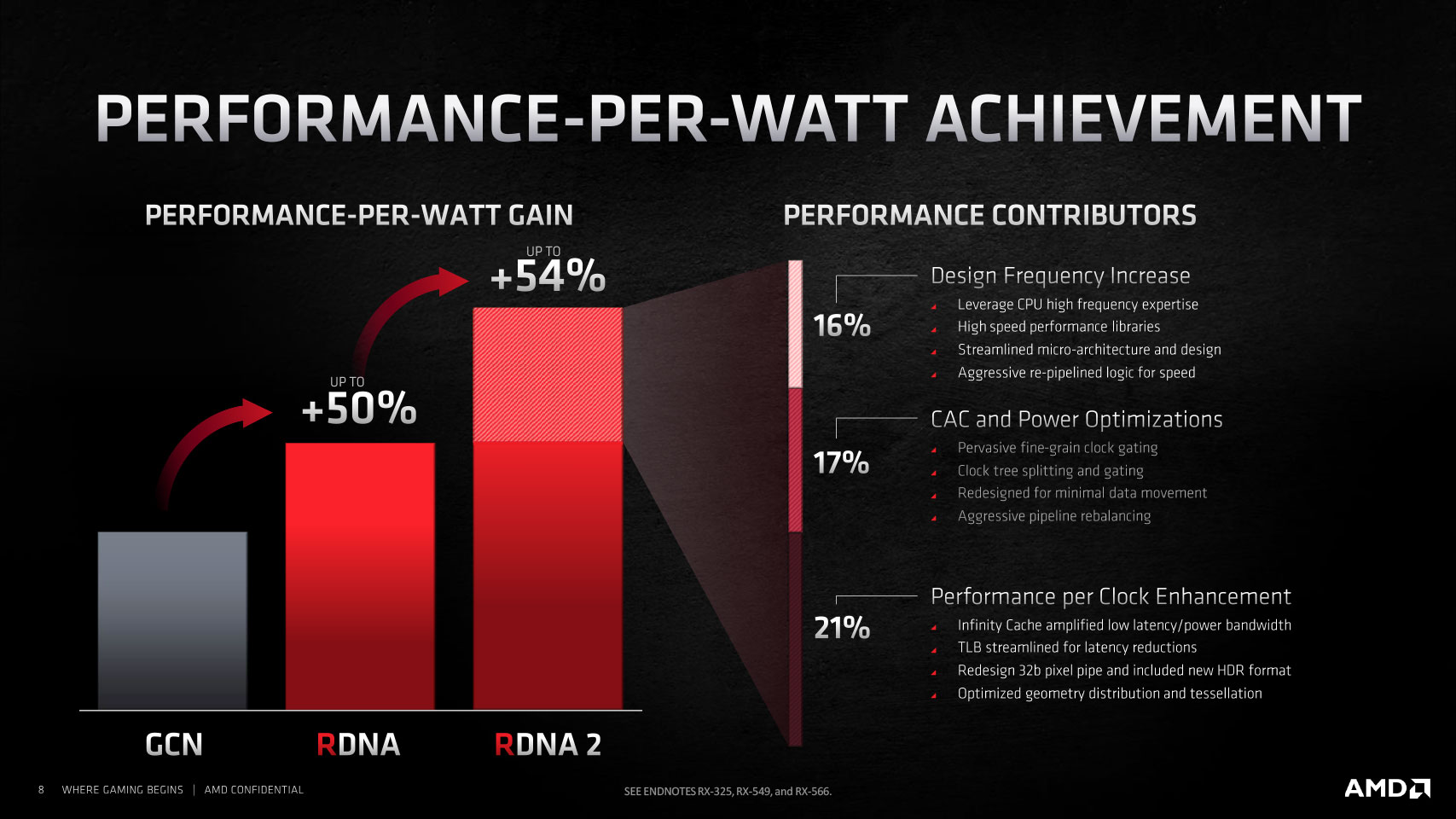
Through new design methodologies and component-level optimization throughout the silicon, along with new power management features, AMD claims to have achieved two breakthroughs that enabled it to double the compute unit counts over the previous generation while staying within a reasonable power envelope. Firstly, the company managed to halve the power draw per CU while adding a 30% increase in engine clocks, which can both be redeemed for performance gain per CU.
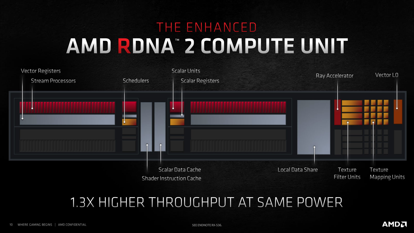
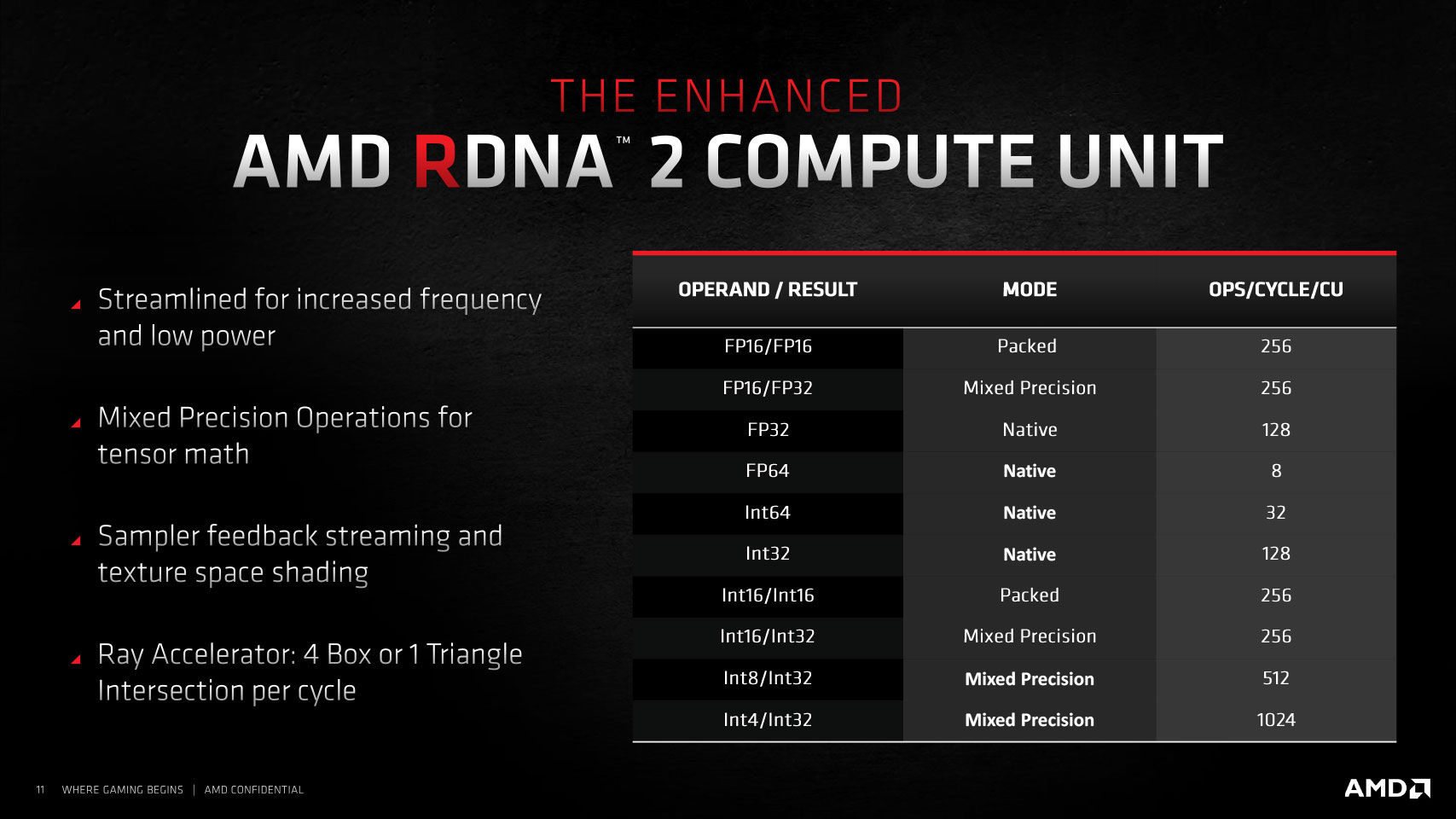
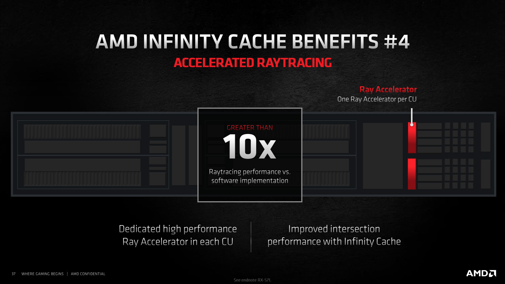
The RDNA2 compute unit is where a bulk of the magic happens. Arranged in groups of two called Dual Compute Units, which share instruction and data caches, the RDNA2 compute unit still packs 64 stream processors (128 per Dual CU), and has been optimized for increased frequencies, new kinds of math precision, new hardware that enable the Sampler Feedback feature, and the all-important Ray Accelerator, a fixed-function hardware component that calculates up to one triangle or four box ray intersections per clock cycle. AMD claims the Ray Accelerator makes intersection performance up to ten times faster than if it were to be performed over compute shaders.

AMD also redesigned the render backends of the GPU from the ground up, towards enabling features such as Variable Rate Shading (both tier-1 and tier-2). The company has doubled ROP counts over "Navi" by giving the chip 128 ROPs. The RX 6800 XT and RX 6900 XT enjoy all 128 ROPs, while the RX 6800 gets 96.
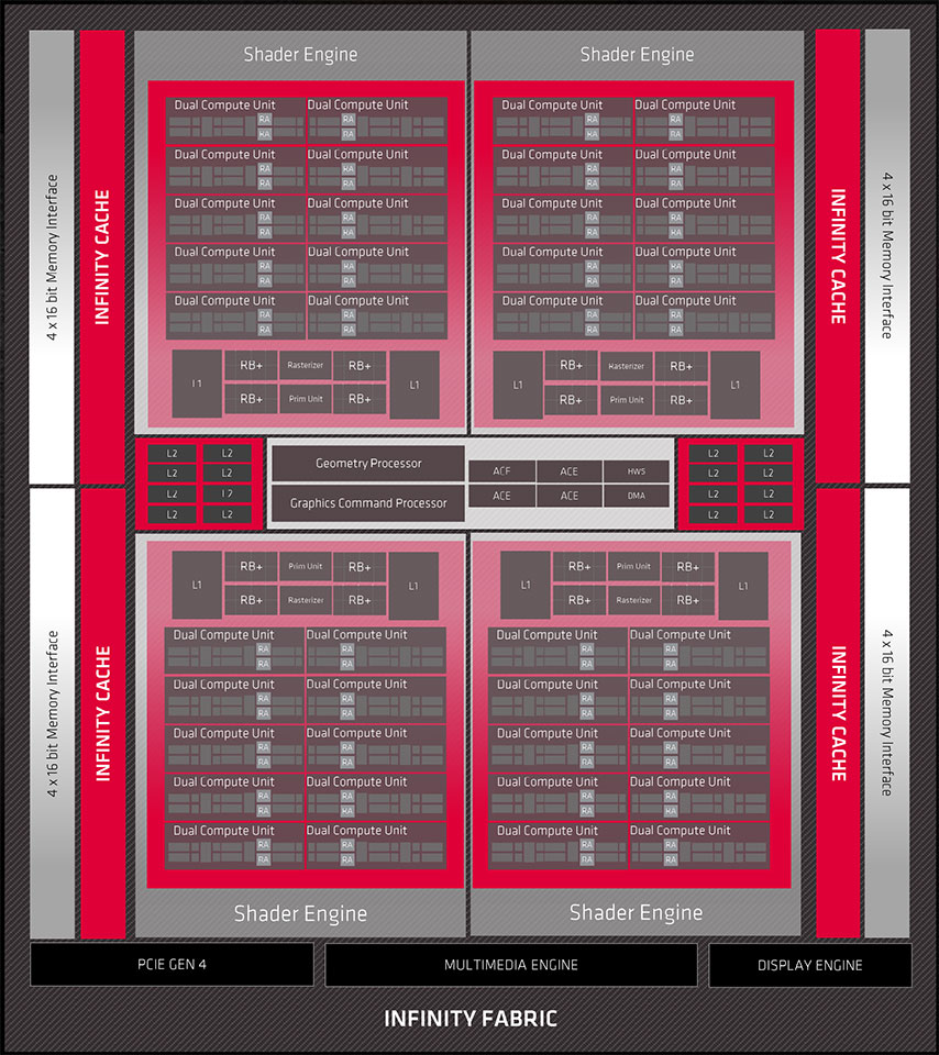
Overall, the "Navi 21" silicon has essentially the same component hierarchy as "Navi 10." The Infinity Fabric interconnect is the link that binds all the components together. At the outermost level, you have the chip's 256-bit GDDR6 memory controllers, a PCI-Express 4.0 x16 host interface, the multimedia- and display engines (which have been substantially updated from RDNA). A notch inside is the chip's 128-megabyte Infinity Cache, which we detail below. This cache is the town-square for the GPU's high-speed 4 MB L2 caches and the Graphics Command Processor, which dispatches the workload among four Shader Engines. Each of these Shader Engines packs 10 RDNA2 Dual Compute Units (or 20 CUs) along with the updated Render Backends and L1 cache. Combined, the silicon has 5,120 stream processors across 80 CUs, 80 Ray Accelerators (1 per CU), 320 TMUs, and 128 ROPs.
The RX 6800 XT is carved out by enabling 72 out of 80 CUs (one disabled Dual CU per Shader Engine), which works out to 4,608 stream processors, 288 TMUs, and an unchanged 128 ROPs. The RX 6800 is further cut down by enabling 60 out of 80 CUs. It's unclear if a full Shader Engine or 10 random Dual CUs have been disabled to accomplish this. The RX 6800 ends up with 3,840 stream processors, 240 TMUs, 60 Ray Accelerators, and 96 ROPs. The RX 6900 XT, which will be launched in December 2020, maxes out the silicon with all 80 CUs enabled.
Infinity Cache, or How AMD is Blunting NVIDIA's G6X Advantage

Despite its lofty design goals and a generational doubling in memory size to 16 GB, the RX 6800 XT and RX 6800 have a rather unimpressive memory setup compared to NVIDIA's RTX 3080 and RTX 3090. That is, at least on paper, with just a 256-bit bus width and JEDEC-standard 16 Gbps GDDR6, which works out to 512 GB/s raw bandwidth. NVIDIA has increased bus widths to 320-bit and 384-bit, and innovated 19–19.5 Gbps GDDR6X memory to go with its cards, offering bandwidth rivaling those of 4096-bit HBM2 setups. Memory compression secret-sauce can at best increase effective bandwidth by a high single-digit percent.


AMD took a frugal approach to this problem, not wanting to invest in expensive HBM+interposer based solutions, which would throw the overall GPU's production costs way off balance. It looked at how AMD's "Zen" processor team leveraged large last-level caches on EPYC processors to significantly improve performance and carried the idea over to the GPU. About 20% the "Navi 21" silicon die area now holds what AMD calls the "Infinite Cache," which is really just a new L3 cache that is 128 MB in size and talks to the GPU's four shader engines at 1024 bits per pin, per cycle. This cache has an impressive bandwidth of 2 TB/s and can be used as a victim cache by the 4 MB L2 caches of the four shader engines.


The physical media of Infinity Cache is the same class of SRAM used for the L3 cache on "Zen" processors. It offers four times the density of 4 MB L2 caches, lower bandwidth in comparison, but four times the bandwidth over GDDR6. It also significantly reduces energy consumption, by 1/6th for the GPU to fetch a byte of data compared to doing so from GDDR6 memory. I'm sure the questions on your mind are what difference 128 MB makes and why no one has done this earlier.
To answer the first question, even with just 128 MB spread across two slabs of 64 MB, each, Infinity Cache takes up roughly 20% of the die area of the "Big Navi" silicon, and AMD's data has shown that much of the atomic workloads involved in raytracing and raster operations are bandwidth-intensive rather than memory-size intensive. Having a 128 MB fast victim cache running at extremely low latencies (compared to DRAM) helps. As for why AMD didn't do this earlier, it's only now that there's an alignment of circumstances where the company can afford to go with a fast 128 MB victim cache as opposed to just cramming in more CUs to get comparable levels of performance, but for less power consumption—as a storage device rather than a logic device, spending 20% of the die area on Infinity Cache instead of 16 more CUs does result in power savings.
Apr 19th, 2024 20:44 EDT
change timezone
Latest GPU Drivers
New Forum Posts
- USB C to USB A hub (42)
- The Official Linux/Unix Desktop Screenshots Megathread (688)
- GTX 1060 6GB ASUS GPU Shuts Down after 5min of Gaming (3)
- Official Board Game Discussion (0)
- AMD RX 7000 series GPU Owners' Club (1068)
- I just succesfully baked DDR4 (69)
- I9 13890HX undervolting Suggestions (4)
- Undervolting Dell XPS 14 9440 is it possible? (7)
- Share your AIDA 64 cache and memory benchmark here (2884)
- Roccat Kone AIMO has developed a double left click, when I click it once. Any fix out there? (34)
Popular Reviews
- Horizon Forbidden West Performance Benchmark Review - 30 GPUs Tested
- Fractal Design Terra Review
- Corsair 2000D Airflow Review
- Thermalright Phantom Spirit 120 EVO Review
- Minisforum EliteMini UM780 XTX (AMD Ryzen 7 7840HS) Review
- Creative Pebble X Plus Review
- FiiO KB3 HiFi Mechanical Keyboard Review - Integrated DAC/Amp!
- ASUS GeForce RTX 4090 STRIX OC Review
- NVIDIA GeForce RTX 4090 Founders Edition Review - Impressive Performance
- ASUS GeForce RTX 4090 Matrix Platinum Review - The RTX 4090 Ti
Controversial News Posts
- Sony PlayStation 5 Pro Specifications Confirmed, Console Arrives Before Holidays (111)
- NVIDIA Points Intel Raptor Lake CPU Users to Get Help from Intel Amid System Instability Issues (102)
- US Government Wants Nuclear Plants to Offload AI Data Center Expansion (98)
- AMD "Strix Halo" Zen 5 Mobile Processor Pictured: Chiplet-based, Uses 256-bit LPDDR5X (84)
- Windows 10 Security Updates to Cost $61 After 2025, $427 by 2028 (82)
- Developers of Outpost Infinity Siege Recommend Underclocking i9-13900K and i9-14900K for Stability on Machines with RTX 4090 (82)
- TechPowerUp Hiring: Reviewers Wanted for Motherboards, Laptops, Gaming Handhelds and Prebuilt Desktops (72)
- Intel Realizes the Only Way to Save x86 is to Democratize it, Reopens x86 IP Licensing (70)