 112
112
AMD Radeon RX 6800 Review
Test Setup »High-Resolution PCB Pictures
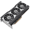
These pictures are for the convenience of volt modders and people who would like to see all the finer details on the PCB. Feel free to link back to us and use these in your articles or forum posts.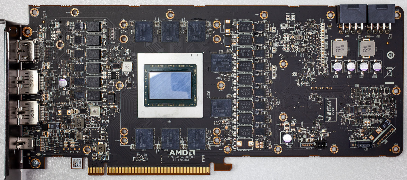
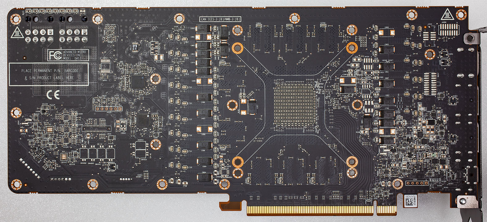
High-res versions are also available (front, back).
Circuit Board (PCB) Analysis

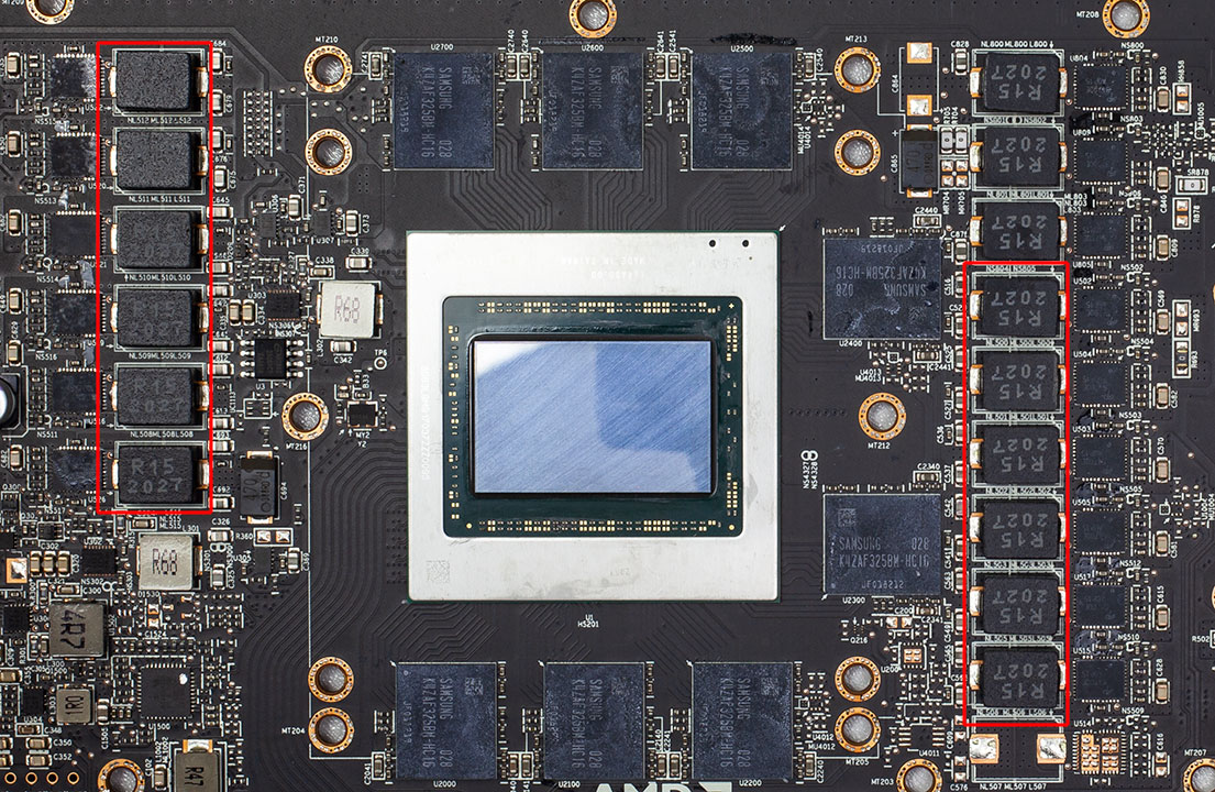
AMD is using a 12-phase GPU VRM design, which is powered by an expensive Infineon XDPE132G5D 16-phase VRM controller. For GPU voltage, a 12-phase VRM configuration is installed. Surprisingly, this is the same VRM design as on the RTX 6800 XT.

AMD is using Alpha & Omega Semiconductor DrMOS components throughout the VRM. This is a difference to the XT, which uses International Rectifier DrMOS chips.
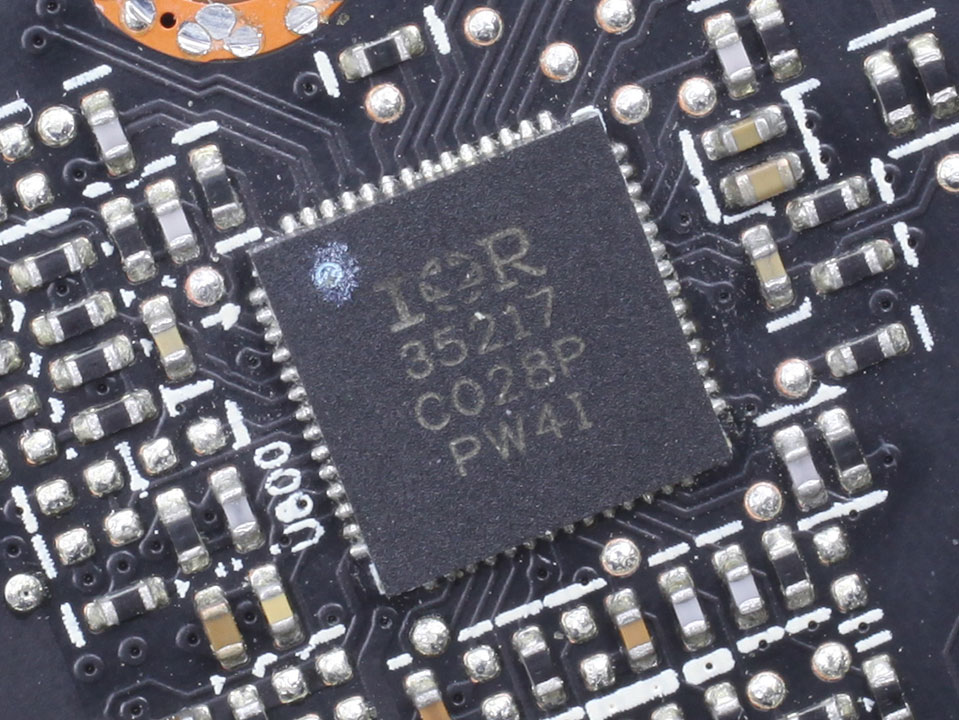

Memory voltage uses a 3-phase design controlled by an International Rectifier IR35217 controller.

The GDDR6 chips are made by Samsung, carry the model number "K4ZAF325BM-HC16," and are rated to run at 16 Gbps.

Built on the same TSMC N7 (7 nm) node as "Navi 10," the "Navi 21" silicon is spread across a 519.8 mm² die area and packs 26.8 billion transistors. The pinkish-red tinge we saw on the "Navi 10" is gone.
Apr 25th, 2024 00:38 EDT
change timezone
Latest GPU Drivers
New Forum Posts
- What's your latest tech purchase? (20337)
- The Official Linux/Unix Desktop Screenshots Megathread (694)
- XFX RX470 8GB no video and error 43 (27)
- (Anti) SFF fun house (348)
- Cinebench crashed my PC. My Wi-Fi stopped working, and I keep getting a "Please wait" screen when I boot up my PC. (31)
- im new to throttelstop and i think i messed it up by copying others any hints would be very much aprreciated (1)
- Aida64 cache mem OC (7)
- I am getting artifacting when I change Windows security settings. Is my GPU failing, or is this just a Windows issue? (10)
- Is there a technical reason that Windows 11 doesn't have built into it battery charge limitation? (42)
- The TPU UK Clubhouse (24783)
Popular Reviews
- Fractal Design Terra Review
- Thermalright Phantom Spirit 120 EVO Review
- Corsair 2000D Airflow Review
- Minisforum EliteMini UM780 XTX (AMD Ryzen 7 7840HS) Review
- ASUS GeForce RTX 4090 STRIX OC Review
- NVIDIA GeForce RTX 4090 Founders Edition Review - Impressive Performance
- ASUS GeForce RTX 4090 Matrix Platinum Review - The RTX 4090 Ti
- MSI GeForce RTX 4090 Suprim X Review
- MSI GeForce RTX 4090 Gaming X Trio Review
- Gigabyte GeForce RTX 4090 Gaming OC Review
Controversial News Posts
- Sony PlayStation 5 Pro Specifications Confirmed, Console Arrives Before Holidays (116)
- NVIDIA Points Intel Raptor Lake CPU Users to Get Help from Intel Amid System Instability Issues (106)
- AMD "Strix Halo" Zen 5 Mobile Processor Pictured: Chiplet-based, Uses 256-bit LPDDR5X (101)
- US Government Wants Nuclear Plants to Offload AI Data Center Expansion (98)
- Windows 10 Security Updates to Cost $61 After 2025, $427 by 2028 (84)
- Developers of Outpost Infinity Siege Recommend Underclocking i9-13900K and i9-14900K for Stability on Machines with RTX 4090 (84)
- TechPowerUp Hiring: Reviewers Wanted for Motherboards, Laptops, Gaming Handhelds and Prebuilt Desktops (78)
- AMD's RDNA 4 GPUs Could Stick with 18 Gbps GDDR6 Memory (73)