 191
191
AMD Radeon RX 6900 XT Review - The Biggest Big Navi
Test Setup »High-resolution PCB Pictures
These pictures are for the convenience of volt modders and people who would like to see all the finer details on the PCB. Feel free to link back to us and use these in your articles or forum posts.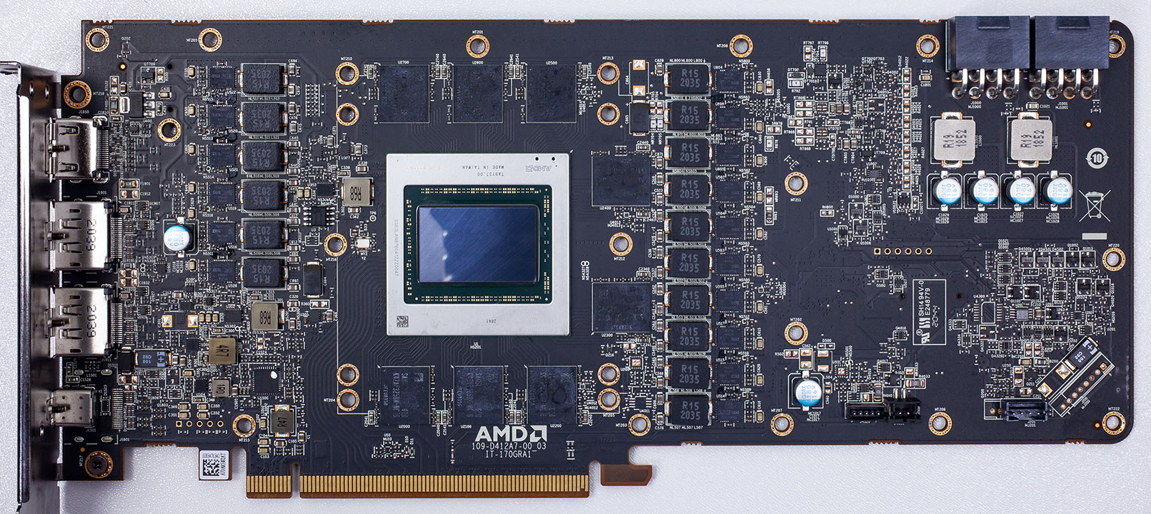

High-res versions are also available (front, back).
Circuit Board (PCB) Analysis
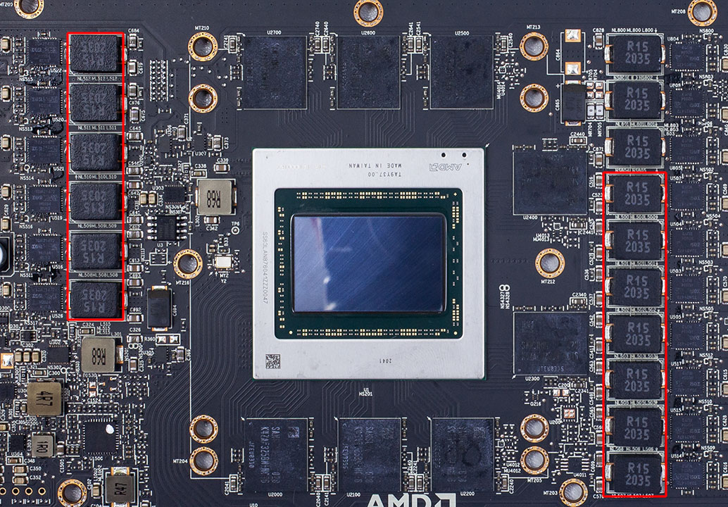

AMD is using a 13-phase GPU VRM design, which is powered by an expensive Infineon XDPE132G5D 16-phase VRM controller. This is one additional phase compared to the RX 6800 XT.

AMD is using International Rectifier TDA21472 DrMOS components on the Radeon RX 6900 XT.


Memory voltage uses a 3-phase design controlled by an International Rectifier IR35217 controller.

AMD "Navi 21" relies on an external USB 3.2 controller for the USB-C port, supplied by Cypress Semiconductor and labeled "CYPD5137-40LQXI." This controller puts out 10 Gbps USB 3.2 Gen 2, DisplayPort passthrough, and 27 W power delivery.

The GDDR6 chips are made by Samsung, carry the model number "K4ZAF325BM-HC16," and are rated to run at 16 Gbps.

Built on the same TSMC N7 (7 nm) node as Navi 10, the Navi 21 silicon is spread across a 519.8 mm² die-area and packs 26.8 billion transistors. The pinkish-red tinge we saw on the "Navi 10" is gone.
Apr 26th, 2024 02:59 EDT
change timezone
Latest GPU Drivers
New Forum Posts
- Best SSD for system drive (82)
- What phone you use as your daily driver? And, a discussion of them. (1484)
- What's your latest tech purchase? (20342)
- AMD RX 7000 series GPU Owners' Club (1087)
- im new to throttelstop and i think i messed it up by copying others any hints would be very much aprreciated (3)
- Horizontal black lines popping up on my screen? (4)
- Which new games will you be buying? (316)
- Alphacool CORE 1 CPU block - bulging with danger of splitting? (20)
- Black screen after muting (5)
- What are you playing? (20530)
Popular Reviews
- Fractal Design Terra Review
- Thermalright Phantom Spirit 120 EVO Review
- Corsair 2000D Airflow Review
- ASUS GeForce RTX 4090 STRIX OC Review
- NVIDIA GeForce RTX 4090 Founders Edition Review - Impressive Performance
- ASUS GeForce RTX 4090 Matrix Platinum Review - The RTX 4090 Ti
- MSI GeForce RTX 4090 Suprim X Review
- Gigabyte GeForce RTX 4090 Gaming OC Review
- MSI GeForce RTX 4090 Gaming X Trio Review
- MSI GeForce RTX 4090 Suprim Liquid X Review
Controversial News Posts
- Sony PlayStation 5 Pro Specifications Confirmed, Console Arrives Before Holidays (117)
- Windows 11 Now Officially Adware as Microsoft Embeds Ads in the Start Menu (112)
- NVIDIA Points Intel Raptor Lake CPU Users to Get Help from Intel Amid System Instability Issues (106)
- AMD "Strix Halo" Zen 5 Mobile Processor Pictured: Chiplet-based, Uses 256-bit LPDDR5X (101)
- US Government Wants Nuclear Plants to Offload AI Data Center Expansion (98)
- AMD's RDNA 4 GPUs Could Stick with 18 Gbps GDDR6 Memory (88)
- Developers of Outpost Infinity Siege Recommend Underclocking i9-13900K and i9-14900K for Stability on Machines with RTX 4090 (85)
- Windows 10 Security Updates to Cost $61 After 2025, $427 by 2028 (84)