 135
135
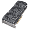
AMD Radeon RX 7900 XT Review
Architecture »Introduction
The new RDNA 3 graphics architecture releases today, and leading from the top are the new Radeon RX 7900 XT (in this review), and the RX 7900 XTX flagship, which we've also reviewed today. Both these graphics cards are designed to take the fight to NVIDIA's high-end: the GeForce RTX 40-series "Ada," but at highly competitive prices. The RX 7900 XT from this review targets a slightly lower price-point than the RX 7900 XTX flagship, while being designed for the exact same class of gaming—4K Ultra HD maxed out with ray tracing. The new RDNA 3 architecture promises to repeat the 50% leap in performance/Watt that made it possible for AMD to return to the high-end graphics segment with their RX 6000 series RDNA2.

The company still believes that Moore's Law exists, and that it requires efficiently utilizing the various foundry nodes to optimize cost. This is basically what AMD does in the CPU space, something it debuted with the Ryzen 3000 series and 2nd Gen EPYC processors. The CPU cores are built on the latest node, while the memory controller isn't. In the same way, the stream processors and other number crunching machinery of the Shader Engines are built on a centralized Graphics Compute Die (GCD) that's fabricated on the latest 5 nm EUV foundry node; while the Infinity Cache memory, memory controllers, and GDDR6 PHY, are pushed to multiple Memory Cache Dies (MCDs), built on the slightly older 6 nm node. The "Navi 31" silicon on which the RX 7900 series is based, features six of these, and hence has a 384-bit wide memory interface. Five of these are enabled on the RX 7900 XT, hence it ends up with a 320-bit memory interface. Each MCD has a 16 MB piece of the GPU's 96 MB Infinity Cache, the RX 7900 XT gets 80 MB of it.
AMD carved the Radeon RX 7900 XT in this review from the "Navi 31" GPU, by enabling 84 out of 96 RDNA 3 compute units physically present on the silicon, and 5 out of 6 MCDs. This results in hardware specs of 5,376 (out of 6,144) stream processors, 336 (out of 384) TMUs, the chip's full 192 ROP count, and a 320-bit GDDR6 memory interface, which runs 20 GB of 20 Gbps memory, resulting in an impressive 800 GB/s memory bandwidth.
The RDNA 3 graphics architecture introduced dual issue-rate compute units, with a high degree of optimization in the way idle SIMD resources are utilized, support for newer math formats, and a new AI accelerator that retasks the SIMD resources for matrix math functions. Together, these optimizations produce a 17% IPC uplift over the RDNA2 CU. There are 96 CUs on the silicon, which work out to 6,144 stream processors. The architecture also sees an increase in engine clocks, and a decoupling of the shader clock speeds to those of the GPU's Front End, which operates at a 10-15% higher frequency. The most striking aspect of the RDNA 3 architecture is that the typical board power of these GPUs is well contained, with the RX 7900 XTX rated at just 350 W, and the RX 7900 XT at 315 W—both of which can be fed by just two 8-pin PCIe power connectors, and cooled by solutions much smaller than those found on the competing NVIDIA GeForce RTX 4080 or RTX 4090 "Ada."
AMD is transferring the costs saved with its chiplet architecture over to customers, by aggressively pricing the Radeon RX 7900 XT at $900. Its bigger sibling, the RX 7900 XTX, goes for just $1,000. Compared to these, the NVIDIA offerings are quite expensive, with the RTX 4080 priced at $1,200 and the flagship RTX 4090 at $1,600. What's more, the RX 7900 XT has a typical power of just 315 W, and makes do with two conventional 8-pin PCIe power connectors, and the reference board design by AMD is as compact as the RTX 3080 Founders Edition, making it friendly with even some SFF cases. In this review, we compare the RX 7900 XT with its segment rivals, as well as a small but growing selection of graphics cards, on our swanky new 13900K-based VGA test-bench.
| Price | Cores | ROPs | Core Clock | Boost Clock | Memory Clock | GPU | Transistors | Memory | |
|---|---|---|---|---|---|---|---|---|---|
| RTX 3070 | $500 | 5888 | 96 | 1500 MHz | 1725 MHz | 1750 MHz | GA104 | 17400M | 8 GB, GDDR6, 256-bit |
| RTX 3070 Ti | $600 | 6144 | 96 | 1575 MHz | 1770 MHz | 1188 MHz | GA104 | 17400M | 8 GB, GDDR6X, 256-bit |
| RX 6800 | $510 | 3840 | 96 | 1815 MHz | 2105 MHz | 2000 MHz | Navi 21 | 26800M | 16 GB, GDDR6, 256-bit |
| RX 6800 XT | $650 | 4608 | 128 | 2015 MHz | 2250 MHz | 2000 MHz | Navi 21 | 26800M | 16 GB, GDDR6, 256-bit |
| RTX 3080 | $750 | 8704 | 96 | 1440 MHz | 1710 MHz | 1188 MHz | GA102 | 28000M | 10 GB, GDDR6X, 320-bit |
| RTX 3080 Ti | $950 | 10240 | 112 | 1365 MHz | 1665 MHz | 1188 MHz | GA102 | 28000M | 12 GB, GDDR6X, 384-bit |
| RX 6900 XT | $700 | 5120 | 128 | 2015 MHz | 2250 MHz | 2000 MHz | Navi 21 | 26800M | 16 GB, GDDR6, 256-bit |
| RX 6950 XT | $800 | 5120 | 128 | 2100 MHz | 2310 MHz | 2250 MHz | Navi 21 | 26800M | 16 GB, GDDR6, 256-bit |
| RTX 3090 | $950 | 10496 | 112 | 1395 MHz | 1695 MHz | 1219 MHz | GA102 | 28000M | 24 GB, GDDR6X, 384-bit |
| RX 7900 XT | $900 | 5376 | 192 | 2000 MHz | 2400 MHz | 2500 MHz | Navi 31 | 57700M | 20 GB, GDDR6, 320-bit |
| RTX 3090 Ti | $1400 | 10752 | 112 | 1560 MHz | 1950 MHz | 1313 MHz | GA102 | 28000M | 24 GB, GDDR6X, 384-bit |
| RTX 4080 | $1200 | 9728 | 112 | 2205 MHz | 2505 MHz | 1400 MHz | AD103 | 45900M | 16 GB, GDDR6X, 256-bit |
| RX 7900 XTX | $1000 | 6144 | 192 | 2300 MHz | 2500 MHz | 2500 MHz | Navi 31 | 57700M | 24 GB, GDDR6, 384-bit |
| RTX 4090 | $2400 | 16384 | 176 | 2235 MHz | 2520 MHz | 1313 MHz | AD102 | 76300M | 24 GB, GDDR6X, 384-bit |
Apr 30th, 2024 14:20 EDT
change timezone
Latest GPU Drivers
New Forum Posts
- RTX 4090? (24)
- HyperX mechanical keyboards (5)
- i7-1355U (14)
- Using software on second monitor (0)
- Would you guys be ok with 70C idle temp on NVME storage. (2)
- problem with my 7900xtx (12)
- Current Sales, Bundles, Giveaways (10212)
- Looking for recommendations to upgrade my ap201 (10)
- Is there a formula to help normalize temperature testing when ambient is variable? (9)
- Using science and technology to cure tinnitus (ear ringing) (35)
Popular Reviews
- Ugreen NASync DXP4800 Plus Review
- HYTE THICC Q60 240 mm AIO Review
- Team Group T-Force Vulcan ECO DDR5-6000 32 GB CL38 Review
- MOONDROP x Crinacle DUSK In-Ear Monitors Review - The Last 5%
- Upcoming Hardware Launches 2023 (Updated Feb 2024)
- Thermalright Phantom Spirit 120 EVO Review
- AMD Ryzen 7 7800X3D Review - The Best Gaming CPU
- FiiO K19 Desktop DAC/Headphone Amplifier Review
- ASUS Radeon RX 7900 GRE TUF OC Review
- Alienware Pro Wireless Gaming Keyboard Review
Controversial News Posts
- Intel Statement on Stability Issues: "Motherboard Makers to Blame" (182)
- Windows 11 Now Officially Adware as Microsoft Embeds Ads in the Start Menu (156)
- Sony PlayStation 5 Pro Specifications Confirmed, Console Arrives Before Holidays (117)
- AMD's RDNA 4 GPUs Could Stick with 18 Gbps GDDR6 Memory (108)
- NVIDIA Points Intel Raptor Lake CPU Users to Get Help from Intel Amid System Instability Issues (106)
- AMD "Strix Halo" Zen 5 Mobile Processor Pictured: Chiplet-based, Uses 256-bit LPDDR5X (103)
- US Government Wants Nuclear Plants to Offload AI Data Center Expansion (98)
- TechPowerUp Hiring: Reviewers Wanted for Motherboards, Laptops, Gaming Handhelds and Prebuilt Desktops (90)