 228
AMD Radeon RX Vega 64 8 GB Review
(228 Comments) »Introduction

AMD's ambitious "Vega" graphics architecture finally completes its long and winding journey into the hands of gamers and enthusiasts, as the Radeon RX Vega series. The architecture made its debut with the "prosumer" segment Radeon Pro Vega Frontier Edition earlier this year, followed by the professional-segment Radeon Pro WX9100 and Radeon Instinct MI25 GPU-compute accelerator for machine-intelligence applications.
Vega's journey into the consumer segment looks longer than it actually is because AMD hasn't launched a high-end GPU in over two years, since its mid-2015 launch of the Radeon R9 Fury series. Its much-hyped "Polaris" architecture could only power products as fast as the upper-mainstream Radeon RX 480 when it came out in mid-2016, competing with NVIDIA's mid-range GP106 silicon powering the GTX 1060 series, leaving no real competitor to the GTX 1080 and GTX 1070. Consumers at the time were hoping for a grand Vega launch by Holiday 2016, but were made to wait another two quarters. The competition wasn't idle all that while. NVIDIA topped its GTX 1080 launch with faster GTX 1080 Ti and TITAN Xp SKUs based on bigger implementations of its "Pascal" GPU architecture; and even refreshed its GTX 1080 and GTX 1060 SKUs with faster memory.

AMD has dropped all of its Vega IP into one silicon codenamed "Vega 10," and all Vega-series products launched so far, including the Radeon RX Vega cards we review today, are based on it. The company is launching two consumer-segment SKUs based on this chip, the Radeon RX Vega 64, which features all 64 of the next-gen compute units physically present on the chip, and the RX Vega 56, which features 56 of them (covered in our second review today). The RX Vega 64 is further being launched in three variants, the standard RX Vega 64 (reference), which we're reviewing today, and two halo SKUs, the RX Vega 64 Limited Edition, featuring a fancy metal cooler shroud and back-plate, and the RX Vega 64 Liquid Cooled featuring a factory-fitted AIO liquid cooler and higher clock speeds.
"Vega 10" is a multi-chip module, much like "Fiji," which powered the R9 Fury series. AMD is referring to its memory as "High Bandwidth Cache," with the operative term being "cache" as opposed to "memory." This is because of sweeping changes the company brought about in the way the GPU addresses video memory.
The RX Vega 64 features all 4,096 stream processors physically present on the chip, which may look like the same count as that of the R9 Fury X, but one has to keep in mind that these stream processors are two generations ahead and are bolstered by a reworked rendering pipeline, higher clock speeds, an improved front-end, and the investments AMD made in improving the memory management; not to mention twice the memory capacity. This, AMD feels, is sufficient to build a high-end GPU that can take on several of NVIDIA's SKUs around the $500 mark.
We put the RX Vega 64 through our vast and modern test bench and have it compete against key NVIDIA SKUs, such as the GTX 1070, GTX 1080, and GTX 1080 Ti; at resolutions as high as 4K Ultra HD. AMD WattMan now includes two additional profiles called "Power Save" and "Turbo", besides the default "Balanced" profile. Also included is a dual BIOS feature with the second BIOS driving the card at lower power levels. These changes prompted us to run the card through our entire testing suite in six different scenarios. If this SKU can tame 4K, it will be the first AMD GPU to do so. According to AMD, you will be able to purchase a Radeon RX Vega 64 with the black reference cooler for $499. The Limited Edition card, which features a different fan shroud but identical performance, is available for $599, though only in a Radeon pack with two games and, optionally, a Ryzen CPU+mobo combo at reduced pricing. AMD's top-end liquid-cooled model is priced at a staggering $699, also in bundle form only, with two games and a Ryzen CPU+mobo+monitor combo (the monitor offer is not available in some regions, including Europe).
| GeForce GTX 980 Ti | Radeon R9 Fury X | GeForce GTX 1070 | Radeon RX Vega 56 | GeForce GTX 1080 | Radeon RX Vega 64 | Radeon RX Vega 64 Liquid | GeForce GTX 1080 Ti | |
|---|---|---|---|---|---|---|---|---|
| Shader Units | 2816 | 4096 | 1920 | 3584 | 2560 | 4096 | 4096 | 3584 |
| ROPs | 96 | 64 | 64 | 64 | 64 | 64 | 64 | 88 |
| Graphics Processor | GM200 | Fiji | GP104 | Vega 10 | GP104 | Vega 10 | Vega 10 | GP102 |
| Transistors | 8000M | 8900M | 7200M | 12500M | 7200M | 12500M | 12500M | 12000M |
| Memory Size | 6 GB | 4 GB | 8 GB | 8 GB | 8 GB | 8 GB | 8 GB | 11 GB |
| Memory Type | GDDR5 | HBM | GDDR5 | HBM2 | GDDR5X | HBM2 | HBM2 | GDDR5X |
| Memory Bus Width | 384 bit | 4096 bit | 256 bit | 2048 bit | 256 bit | 2048 bit | 2048 bit | 352 bit |
| Core Clock | 1000 MHz+ | 1050 MHz | 1506 MHz+ | 1156 MHz+ | 1607 MHz+ | 1274 MHz+ | 1406 MHz+ | 1481 MHz+ |
| Memory Clock | 1750 MHz | 500 MHz | 2002 MHz | 800 MHz | 1251 MHz | 953 MHz | 953 MHz | 1376 MHz |
| Price | $390 | $380 | $350 | $400 | $500 | $500 | $700 | $700 |
Architecture
As we mentioned in the introduction, when the Radeon RX 480 turned out to be an upper-mainstream product in June 2016, consumers half-expected the performance-thru-enthusiast segment "Vega" to launch by the end of the year. That didn't happen. What we got instead were not one, but two media events detailing the "Vega" architecture. On each occasion, we did a special article detailing the press-decks given to us by AMD. Our first article, dated early-January, focused on the broader points of the architecture. Our second article followed close to seven months later, getting into the finer points of the architecture. On this page, we'll summarize the most important content from both presentations.The Radeon RX Vega 64 is based on the "Vega 10" GPU. This is a multi-chip module of a GPU die, and memory stacks, much like its logical predecessor, "Fiji" (R9 Fury X, R9 Nano). The GPU die is built on the 14 nm FinFET process and packs over 12 billion transistors. It's wired to two 32 Gbit HBM2 memory stacks over a 2048-bit wide memory interface, which is half the bus width of "Fiji", but is somewhat made up for with higher clocks. The bandwidth itself is less than that of the R9 Fury, at just 484 GB/s against the Fury's 512 GB/s, but AMD made some sweeping changes to the way in which it addresses memory, which should more than make up for the bandwidth deficit.


Memory management has traditionally been a problem area for AMD's otherwise stellar Graphics CoreNext architecture, and AMD added raw bus width and memory compression to overcome issues that were intrinsic to the architecture. With Vega, AMD is addressing those fundamental issues by using a memory concept called "High Bandwidth Cache," with the keyword being "cache." The "Vega" silicon addresses a large virtual-memory space that spans up to 512 TB, a tiny portion of which is physical, in this case the "cache." This allows for the fine-grained movement of data in and out of the virtual-address space based on data "heat" (frequency of access).


The essential hierarchy of the GPU doesn't appear to have changed with "Vega"; however, its designers seem to have made big changes with the front-end and back-ends of the rendering pipeline, while incrementally improving the Compute Units, the number-crunching components that do the heavy lifting.


The newer-generation programmable geometry pipeline provides double the throughput over the previous generation. The Next-Generation Compute Units (NGCUs) are based on the 5th generation Graphics CoreNext architecture and feature support for not just FP16 operations (introduced with "Polaris"), but also primitive 8-bit operations. Bolstered by Rapid Packed Math, each CU can handle up to 512 8-bit operations per clock cycle, and up to 256 16-bit ones. Quite a few of today's effects can be simplified to 16-bit or 8-bit ops, which frees up much of the CU's resources for other ops. Lastly, there is an improved pixel engine featuring a draw-binning rasterizer.


The "Vega 10" silicon features 64 NGCUs, each with 64 stream processors (SP), indivisible SIMD units which total the chip's SP count at 4,096 on the RX Vega 64 and 3,584 on the RX Vega 56. The chip also features 256 texture memory units (TMUs) and 64 ROPs. Its 2048-bit wide HBM2 memory interface holds 8 GB of memory (or high-bandwidth cache) on the Radeon RX Vega 64 and RX Vega 56.
AMD Enhanced Sync
We can safely call the AMD FreeSync technology the victor of the adaptive display-sync-standard war. It beats G-SYNC because it's both easy and free to implement, and has the backing of VESA, the display-standards governing body. AMD is doubling down on adaptive display-sync with a new standard, Enhanced Sync, which is bound to be more successful because it doesn't even need compatibility on the monitor's side, and it works with any digital display connector.
Before we get to the mechanics of Enhanced Sync, here's a quick refresher about V-Sync. Your display has a fixed maximum refresh rate (the rate at which it draws a new frame to make up moving images), while your PC puts out frames to the display at a variable rate, depending on the speed of your hardware. If it puts out frames at a rate slower than your monitor's refresh-rate, you experience stuttering (a noticeably rough video). If it puts out at a higher rate, you experience screen tearing, caused because your GPU is pumping in new frames before your monitor can finish drawing frames at its rate. V-Sync is a feature in which the software limits the rate at which your GPU puts out frames, by syncing it with your display's refresh rate. The result is smooth display, but it results in input lag because your game only takes in the same number of inputs per second as the number of frames it has to draw per second.
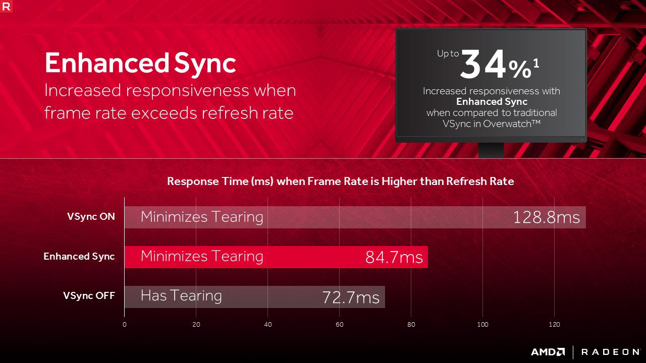

AMD feels that there is a middle path for games that don't have FreeSync-ready displays, and yet want to counter page-tearing at high frame rates or stuttering at low frame rates - hence Enhanced Sync. This is not meant as a replacement, successor, or substitute to FreeSync, but, rather, as its next best thing.
Enhanced Sync counters page tearing by allowing your game to think it has no V-Sync frame-rate caps, thereby taking in more inputs per second while, on the other hand, intelligently culling the frames being sent to the display (and conserving hardware resources in the process), so that the output looks in-sync, without the appearance of lost frames, torn-frames, or other artifacts. Enhanced Sync combats the problem of low frame-rates causing stuttering by allowing for some frame-tearing.
FreeSync
FreeSync provides a novel solution to the problem of low frame rates causing display stutter by keeping your monitor in sync with the frame rate of your game in real time, rather than the other way around. The display's refresh rate is controlled by the source (in this case, your GPU) rather than it having a static refresh rate. When your game's frame rate is higher than the refresh rate of your display, beyond a point, FreeSync allows the game to take in a limitless amount of input, while running the display at its highest refresh rate and culling frames being sent to it. The display's refresh rate keeps in sync with your software fluidly, and hence gives you the appearance of fluid motion, and an uncompromising game-input experience.Our Patreon Silver Supporters can read articles in single-page format.
Nov 15th, 2026 17:10 CST
change timezone
Latest GPU Drivers
New Forum Posts
- Local LLM General Discussion (691)
- WarpCoreBench scores! (54)
- What are you playing? (26223)
- Folding Pie and Milestones!! (10205)
- Asus Rog Maximus Z890 Extreme. (Various questions). (25)
- Power supply noise stops when I move the mouse (9)
- TPU's Nostalgic Hardware Club (22165)
- HP Office Jet 7740 Pro - Supply system problem with replacement cartridge (3)
- Recommendations Wanted - Affordable Enterprise SSD for Boot (9)
- What can the FX 8320 do today? Here is the answer. (59)
Popular Reviews
- AMD Zen 6 Technical Deep Dive
- ASUS ROG Strix B850-I Gaming Wi-Fi7 W Review
- Corsair HX1000i Shift Crystal Review
- Upcoming Hardware Launches 2027 (Updated Nov 2026)
- Montech King 95 3D PRO Review
- NZXT C1200 Platinum Review
- NZXT H7 RGB+ Review
- NZXT H5 Review
- Phantom Blade Zero Performance Benchmark Review - 35 GPUs Tested
- AMD Ryzen 7 9800X3D Review - The Best Gaming Processor
TPU on YouTube
Controversial News Posts
- NVIDIA Co-Founder and CEO Jensen Huang Officially Resigns (422)
- Open Letter Asking NVIDIA to Reinstate Jensen Huang Passes 115,000 Signatures (184)
- OpenAI CEO Argues Home PCs Waste the World's Limited DRAM Supply (152)
- NVIDIA Launches Investigation Into Jensen Huang's Relationship With Suspected Chinese Spy (136)
- Intel "Raptor Lake Next" 16-Core and 20-Core CPUs Surface (130)
- Legendary Game Studio BioWare Shuts Down Following EA Layoffs (104)
- Dell CEO Says the Memory Shortage Will Get Worse in 2027 (95)
- NVIDIA GeForce RTX 50-Series Scheduled for up to $500 Price Hike This Week (89)