 131
131
AMD Radeon RX Vega Preview
(131 Comments) »Introduction
Today, AMD is pulling the curtains off one of its most eagerly awaited products it has ever brought to market. The Vega graphics architecture is without a doubt one of the releases AMD has taken more time in actually delivering, with whispers and semi-announcements of the new high-performance architecture doing the rounds for around two years already. The Vega name comes from α Lyr, a star which may very well be touted as the second most important star in the firmament next to our own sun; however, AMD certainly won't be settling for second best, not when it has been notably absent from the high-performance graphics market for a while now.

Vega breaks away from the iterative improvement on AMD's GCN architecture that we've been seeing for several years now. Incremental upgrades and feature-set augmentations are now paired with specifically designed, never before seen hardware solutions, which the company took two years to perfect and ready for prime time. AMD's investments in High Bandwidth Cache (HBC) and the accompanying High Bandwidth Cache Controller (HBCC); the new programmable geometry pipeline; rapid packed math (rpm), and the new advanced pixel engine are all signs of an AMD that is future-proofing its architecture of today. Vega is arguably the most exotic graphics architecture to date with its slew of finesse-based improvements (like the HBC implementation) and pairing of components (with the ultra-fast HBM2 memory.)
AMD's Vega RX gaming card lineup consists of the following three models, which we will take a detailed look at on the following pages.

AMD Radeon RX Vega 64

The 64 in the RX Vega 64 name signifies the CU count of the GPU. A CU is an indivisible unit of shaders and TMUs that sits inside the GPU. For the Vega architecture, these CUs are called Next Gen Compute Units (NGCU), due to the architectural improvements. Each NGCU features 64 stream processors and four texture mapping units.
After doing the math (64 CUs times 64 shaders per CU), we arrive at a total shader count of 4096 for the Vega 64, which is the same as on the Radeon Fury X (Fiji). GPU clock ranges from from the 1247 MHz base clock up to a 1546 MHz Boost clock, which is higher than on any other graphics card from the company yet. As expected, the card uses HBM 2 memory, which allows bigger memory capacities than HBM1 on Fiji that was limited to 4 GB. With 8 GB, the memory size is a great choice, providing sufficient headroom for tomorrow's games, too. Memory bandwidth is listed at 484 GB/s on a 2048-bit wide memory bus, which translates into a memory clock of 945 MHz.
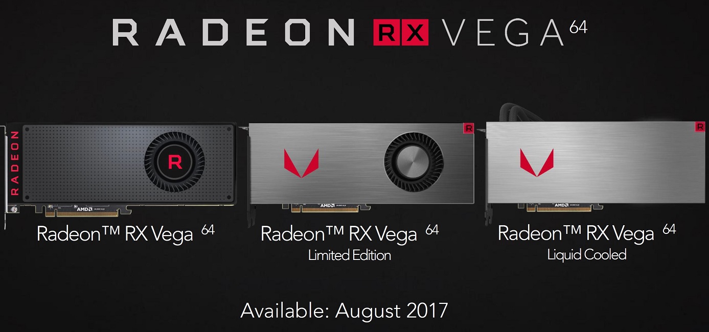
Three variants of the RX Vega 64 will be made available by AMD. Custom boards from AIBs are expected to start in Q3 and into Q4, so right for the Christmas business.

The biggest takeaway here is the $499 price point for the RX Vega 64, at least for the regular edition seen on the left in the image above detailing all three. We confirmed with AMD that the regular edition includes a backplate and dual-BIOS, just like the more expensive versions. AMD is targeting the NVIDIA GeForce GTX 1080 here, mentioning that the market for GPUs priced higher than $500 (USD) is around a million units sold globally per quarter, which might be relatively tiny compared to the rest of the market, but these boards come with better margins.

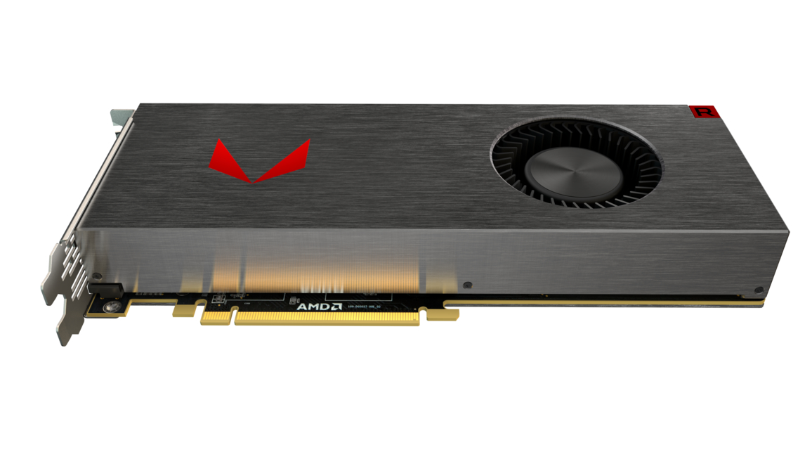

The other two versions of the RX Vega 64 are based off the same PCB, but have different coolers on board. The RX Vega 64 Limited Edition comes with a silver brushed aluminum shroud and LEDs on board, as well as a matching silver metal backplate relative to the presumably plastic backplate on the regular edition. While the looks are different, the cooling performance is exactly the same, due to an identical thermal assembly that is used (only the cooler shroud is different). Also identical are the clock frequencies; the Limited Edition essentially serves as a slightly more premium filler product until the board partners have their own designs ready, after which it will disappear from the market. The renders AMD provided do indicate a directional vane to help guide airflow through a vapor chamber heatsink (not pictured), with the I/O ports on a single row to assist with airflow. We already took a look at these in person here on TechPowerUp, so check them out there. Given TDP and rated core/memory frequencies are identical to the non-limited edition, you are basically paying the extra $50 for the fancier looking cooler as the less expensive version has the same TDP and cooling performance.
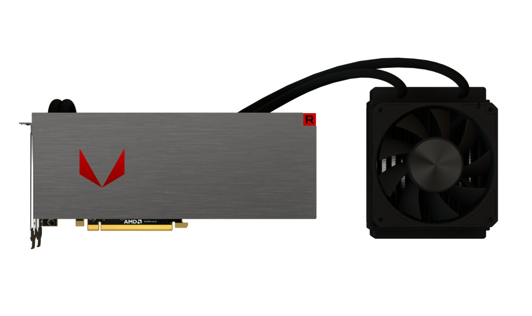

Next up is the Liquid Cooled Edition featuring what appears to be a Cooler Master AIO watercooling solution with possibly a genuine Nidec-Servo high speed Gentle Typhoon fan (or a good copy) on a single 120 mm radiator. The renders provided also indicate that the cooler design from the Radeon Vega Frontier Edition Liquid Cooled card will carry over, with the pump, reservoir/pressure equalizer, and cold plates all mounted onto the PCB allowing for a longer-lasting solution. The watercooling solution also means AMD has gone with increased core clocks to take advantage of the increased 265 W TDP relative to the 220 W on the other two air-cooled editions. The Liquid Cooled Edition will not be available for purchase outside of a bundle - more on that later.

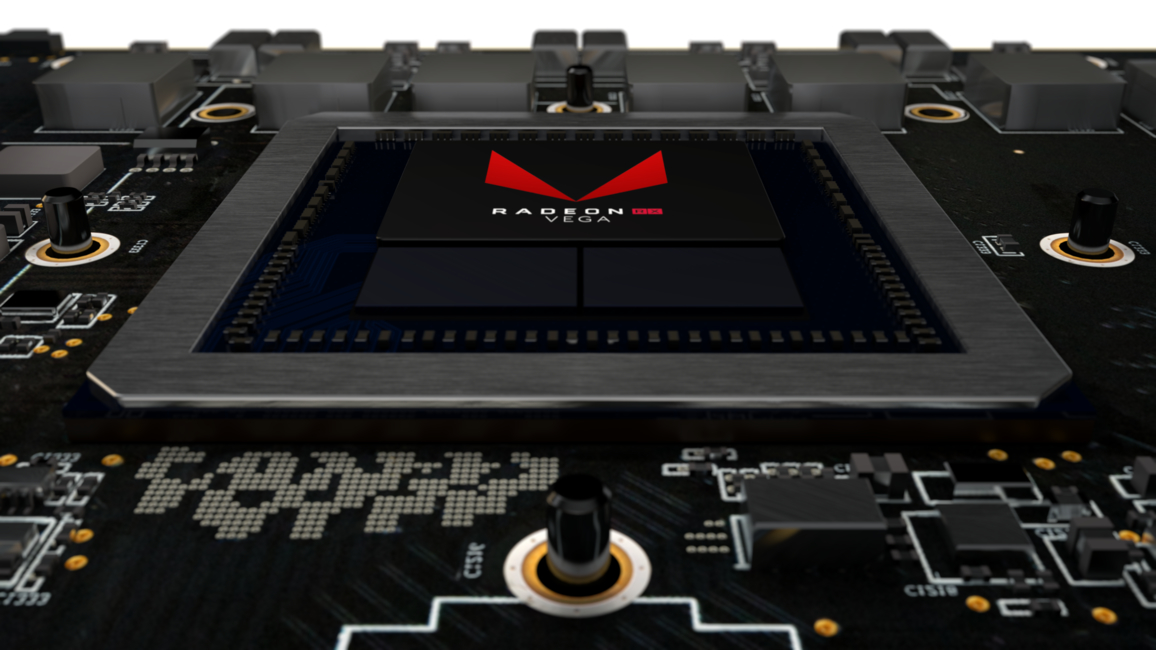


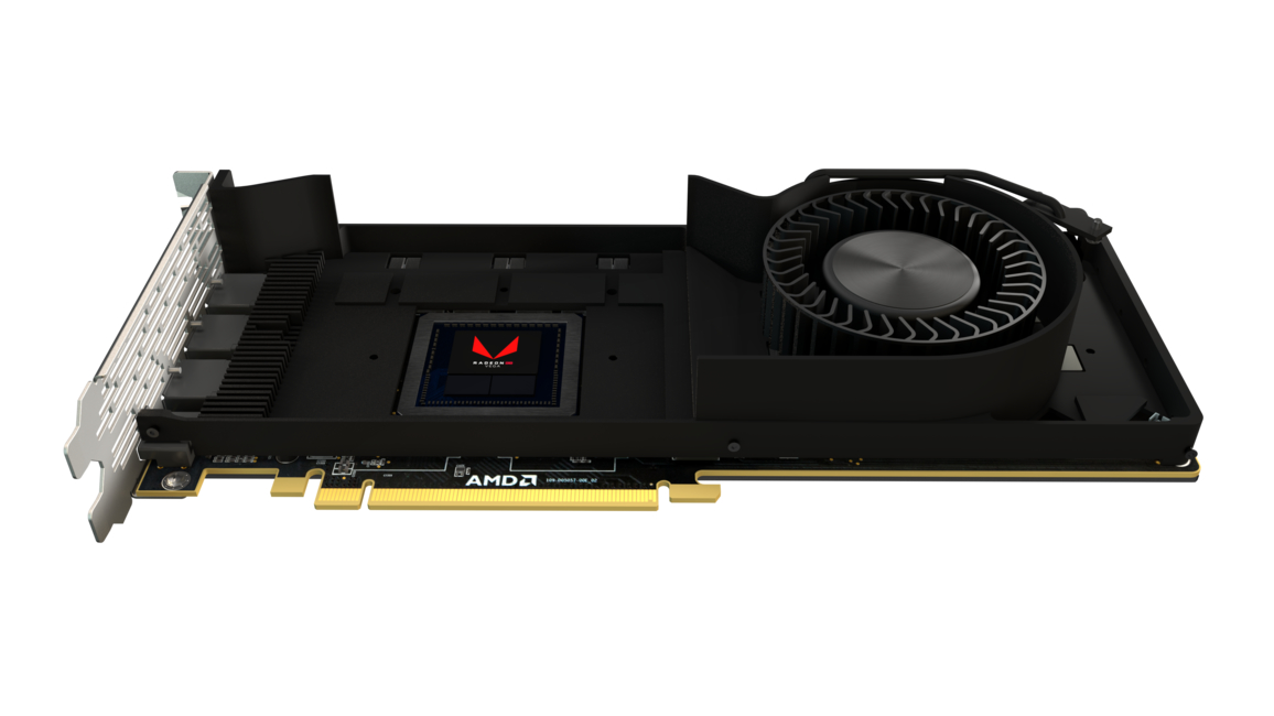
AMD also provided some renders of the PCB with the cooler off, although these are all close-ups around the GPU core. We see the GPU die in the center (which will not have any print or etching on it in real life) and the two HBM stacks below. The power delivery is handled by VRMs soldered around this similar to how we have VRAM modules on non-HBM cards, although we will have to wait until we have a card in hand to get more technical details here. It is likely that the PCB has some available real estate to the right and closer to the 2x8-pin PCIe connectors based on the length of the card, and it is a shame that AMD has not provided a smaller form factor version similar to what they did with the R9 Nano series.
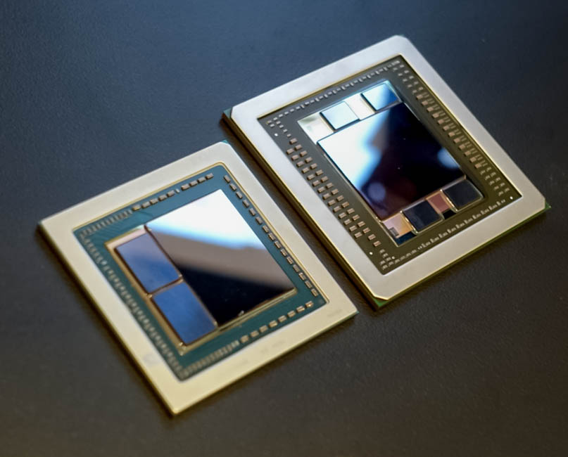
Lastly, we got our hands on the Radeon RX Vega die with the 8 GB HBM2 stack (left), compared to the larger Radeon Fury X GPU with four HBM1 stacks (right). Thus, despite the core packing more transistors with Vega (486 mm^2 with 12.5 billion transistors vs 598 mm^2 with 8.6 billion transistors) and the VRAM size having been doubled, the entire package takes up slightly less space, which further adds to the PCB's length being a sore point here.
Preliminary Performance
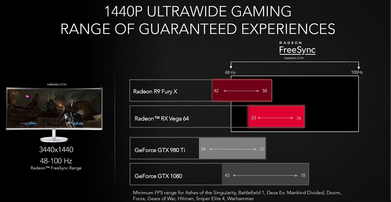
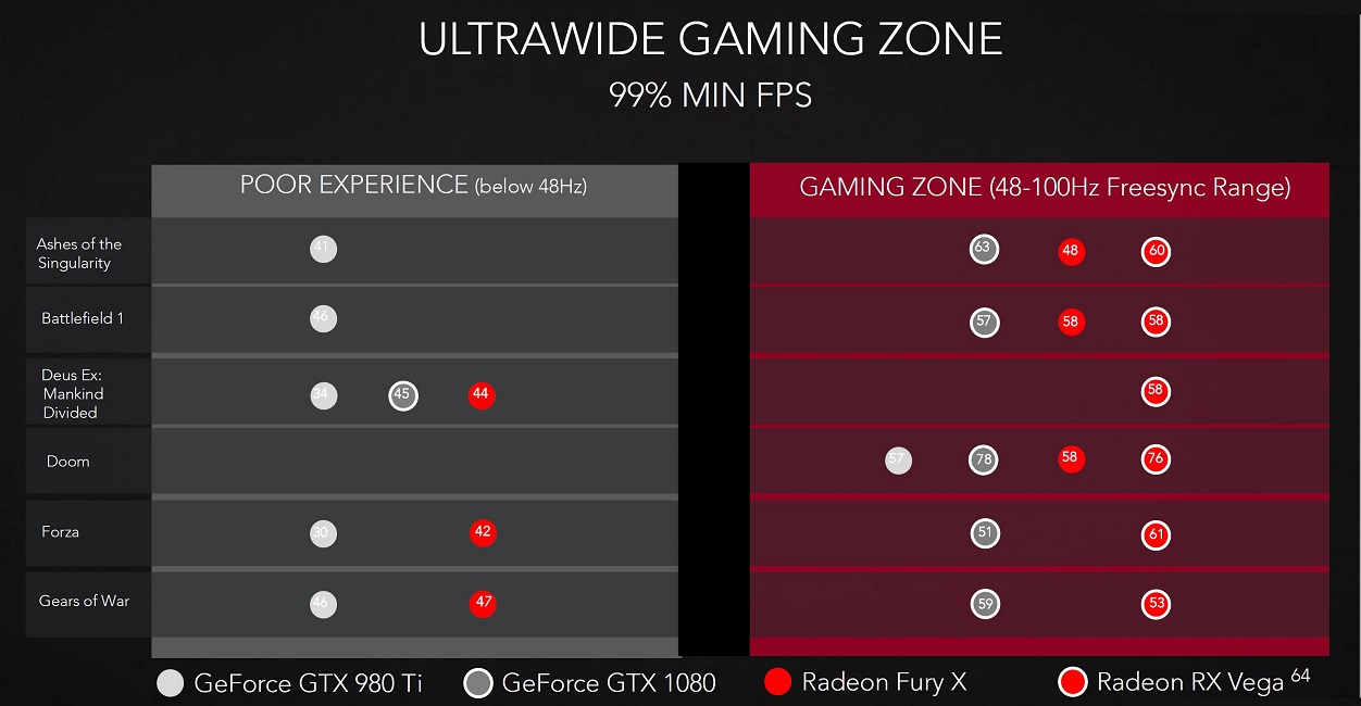
AMD provided some internal performance numbers from their own testing, so do as always take these with a grain of salt. These tests were done on an Intel Core i7-7700K at 4.2 GHz, 16 GB of DDR4-3000 MHz RAM, and with the latest available drivers for the AMD and NVIDIA GPUs at the time. Refer to the complete slide deck at the end for full testing information, but there was nothing that caught our eye otherwise. The chosen games were all running on DX12 or Vulkan APIs, and the order of the four GPUs being presented is certainly on purpose, but looking purely at the numbers and no more, it appears that the RX Vega 64 trades blows with the NVIDIA GeForce GTX 1080 at stock settings under WQHD (21:9, 1440p). With no mention on the exact GPU and memory frequencies, we definitely recommend holding off until independently tested reviews are out.
With those slides, AMD also wants to highlight that with higher minimum FPS than the GTX 1080 and Freesync, the RX Vega 64 will deliver a perfectly smooth gaming experience - guaranteed.


The story continues with 4K gaming, except that the game set is different here, and once again, we see the RX Vega 64 winning some and losing some, relative to the GTX 1080. Compared to the R9 Fury X, we see an average increase of ~35% FPS in these titles. Missing from the comparison here is NVIDIA's current GTX 1080 Ti flagship, which is the best choice for 4K gaming right now, although at higher pricing. These performance numbers are presumably from the air-cooled editions, so the $499 SKU should get you the same performance as reported here.
Before we head to the next page, a note on the method of comparison here: AMD is using FreeSync ranges of specific monitors as a way to quantify what constitutes a poor gaming experience from a better one. Missing conveniently are the GSync monitors released and upcoming with a similar, if not larger, range for variable refresh rate operation. However, as we will see soon, AMD has an answer to that too, but it may not be what you think.
Our Patreon Silver Supporters can read articles in single-page format.
Apr 26th, 2024 15:04 EDT
change timezone
Latest GPU Drivers
New Forum Posts
- Best SSD for system drive (88)
- What phone you use as your daily driver? And, a discussion of them. (1486)
- Windows 11 General Discussion (5024)
- hacked (75)
- XFX RX470 8GB no video and error 43 (30)
- looking to build a new system and im considering asrock brand but i have some doubts/concerns. (0)
- DTS:X APO4 + DTS Interactive for Most Devices [USB Supported] (305)
- The Official Linux/Unix Desktop Screenshots Megathread (702)
- What's your latest tech purchase? (20352)
- im new to throttelstop and i think i messed it up by copying others any hints would be very much aprreciated (5)
Popular Reviews
- HYTE THICC Q60 240 mm AIO Review
- MOONDROP x Crinacle DUSK In-Ear Monitors Review - The Last 5%
- Alienware Pro Wireless Gaming Keyboard Review
- Upcoming Hardware Launches 2023 (Updated Feb 2024)
- Thermalright Phantom Spirit 120 EVO Review
- FiiO K19 Desktop DAC/Headphone Amplifier Review
- ASUS Radeon RX 7900 GRE TUF OC Review
- AMD Ryzen 7 7800X3D Review - The Best Gaming CPU
- RTX 4090 & 53 Games: Ryzen 7 5800X vs Ryzen 7 5800X3D Review
- NVIDIA RTX 4090: 450 W vs 600 W 12VHPWR - Is there any notable performance difference?
Controversial News Posts
- Windows 11 Now Officially Adware as Microsoft Embeds Ads in the Start Menu (129)
- Sony PlayStation 5 Pro Specifications Confirmed, Console Arrives Before Holidays (117)
- NVIDIA Points Intel Raptor Lake CPU Users to Get Help from Intel Amid System Instability Issues (106)
- AMD "Strix Halo" Zen 5 Mobile Processor Pictured: Chiplet-based, Uses 256-bit LPDDR5X (103)
- US Government Wants Nuclear Plants to Offload AI Data Center Expansion (98)
- AMD's RDNA 4 GPUs Could Stick with 18 Gbps GDDR6 Memory (95)
- Developers of Outpost Infinity Siege Recommend Underclocking i9-13900K and i9-14900K for Stability on Machines with RTX 4090 (85)
- Windows 10 Security Updates to Cost $61 After 2025, $427 by 2028 (84)