 223
223
AMD Radeon Vega GPU Architecture
(223 Comments) »Introduction
Vega is the common name of α Lyr, a star located some 25 light years from our Sun, which the scientific community regards as being the "second most important star in the sky after the Sun." Over the centuries, data from observing this star has been used to make great discoveries in the field of astrophysics. It also earned its place among several cultures and mythologies. AMD named its next-generation graphics processor architecture after this majestic, pale-blue celestial body. It is also AMD's most important development by way of high-performance silicon design after the "Zen" micro-architecture on which the company is pinning its resurrection in the CPU market.

"Vega" isn't a fancy name for the 5th generation Graphics CoreNext architecture, a new iteration of AMD's number-crunching machinery inside the GPU, but an entirely new GPU design. The GPUs will still employ GCN compute units, but will augment them with several new components never before featured on AMD GPUs, which will improve the chip's efficiency to cope with complex graphics and general processing workloads.


The idea behind "Vega" is that conventional approaches to making GPUs, so AMD believes, will not be able to cope with emerging workloads. The industry has already made a great leap from years of stagnating at 1080p to 2K and 4K resolutions that demand a proportionate increase in GPU performance. What's more, the workload itself requires optimization at the silicon level, without AMD having to optimize them at the software level through regular driver updates. This means giving the GPU the ability to learn the way a 3D app behaves to have it optimize itself to the app, which isn't easy as the GPU needs a second set of lightning fast memory that works in tandem with the video memory itself.


The GPU also needs expanded geometry processing capabilities to cope with the ever-growing realism in today's photorealistic 3D scenes. To work the tremendous amount of math that goes into it, the GPU needs a new Compute Unit design with added performance. Lastly, it needs an updated pixel-engine that puts it all together to draw the 3D scene. AMD claims to have made big changes to all four areas with "Vega."
In this article, we take a brief stroll through the various changes AMD made to the modern GPU with the "Vega" architecture.
Improved Memory Mangement

Take a good look at the schematic diagram above. It is not a die block diagram, it's not even the layout of the multi-chip module that some of the first "Vega" GPUs will be, but rather illustrates a completely revamped memory architecture which makes sure data moves smoothly in and out of the GPU, and precious resources aren't wasted in fetching data from the host machine. AMD GPUs have traditionally been endowed with vast amounts of memory bandwidth using wide memory bus widths; however, AMD thinks there is room for improvement in the way the GPU juggles data between the host and its local video memory, and that it can no longer simply throw brute memory bandwidth at some fundamental problems.

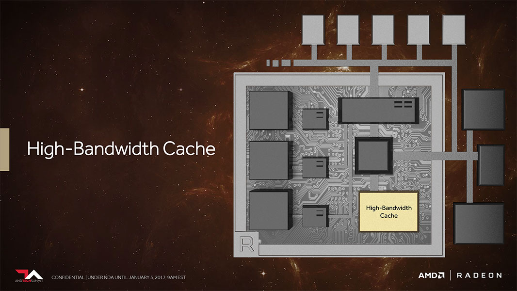
AMD feels there is a disparity between the memory allocation and actual memory access by apps. An app could load into memory resources it finds relevant to the 3D scene being rendered, but not actually access all of it all the time. This disparity eats up precious memory, hogs memory bandwidth, and wastes clock cycles in trying to move data. The graphics driver development team normally collaborates with game developers to minimize this phenomenon and rectify it both through game patches and driver updates. AMD feels something like this can be corrected at the hardware level. AMD calls this "adaptive fine-grained data movement." It is a comprehensive memory allocation pipeline that senses the relevance of data to preemptively move it to the relevant physical memory, or defers access.


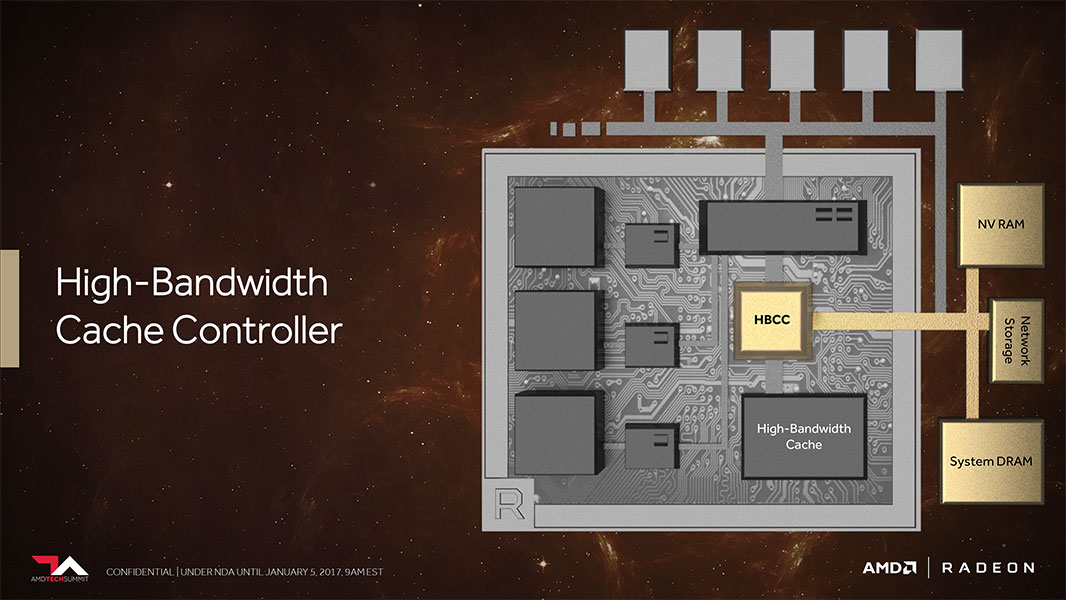
Pulling something like this off requires new hardware components not found on AMD GPUs ever before. It begins with a fast cache memory that sits at a level above the traditional L2 cache, one that is sufficiently large and has extremely low latency. This cache is a separate silicon die that sits on the interposer, the silicon substrate that connects the GPU die to the memory stacks. AMD is calling this the High Bandwidth Memory Cache (HBMC). The GPU's conventional memory controllers won't interface with this cache since a dedicated High Bandwidth Cache Controller (HBCC) on the main GPU die handles it. High Bandwidth Memory Cache isn't the same as the HBM2 memory stacks.
The HBCC has direct access to the other memory along the memory pipeline, including the video memory, system memory, and so on. It has its own 512 TB virtual address space that's isolated / abstract from the machine's general address space. The GPU uses the HBMC to cushion and smooth out data movement between the host machine and the GPU. This approach ensures the GPU has to spend lesser resources on fetching irrelevant data, which greatly improves memory bandwidth utilization. The reason for such a large virtual address space is the same as on the CPU: Adresses can be allocated more efficiently, with the memory-management unit in the GPU managing the virtual-to-physical mapping and also having the ability to move memory pages between storage layers, similar to how the Windows paging file works. Also, you'll notice the little box named "NVRAM." This means the GPU has the ability to directly interface with NAND Flash or 3D X-point SSDs over a localized PCIe connection, which gives it a fast scratchpad for help with processing gargantuan data sets. The "Network" port lets graphics card makers add network PHYs directly onto the card, which would help with rendering farms. This way, AMD is prepping a common silicon for various applications (consumer graphics, professional graphics, and rendering farms).

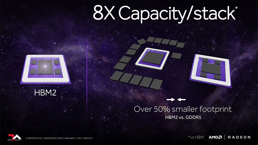
As reported in the news, "Vega" takes advantage of HBM2 memory, which comes with eight times the maximum density per stack and double the bandwidth as HBM1 memory, which debuted with the Radeon R9 Fury X. In theory, you can deploy up to 32 GB of memory across four stacks, doing away with the crippling 4 GB limitation of HBM1.
Next Generation Geometry, Compute, and Pixel Engine


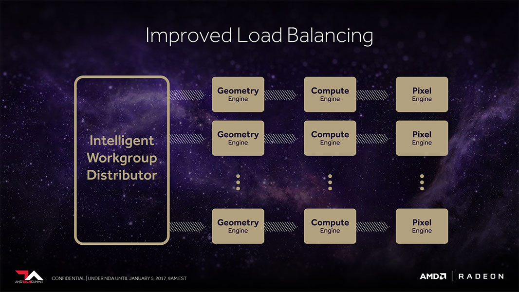
AMD improved the geometry processing machinery available to previous generations with "Vega." The new generation programmable geometry pipeline has over two times the peak throughput per clock. Vega now supports primitive shaders, besides the contemporary vertex and geometry shaders. AMD has also improved the way it distributes workloads between the geometry, compute, and pixel engines. A primitive shader is a new type of low-level shader that gives the developer more freedom to specify all the shading stages they want to use, and run those at a higher rate because they are now decoupled from the traditional DirectX shader pipeline model. While ideally the developer would perform that optimization, AMD also has the ability to use their graphics driver to predefine cases for a game, in which a number of DirectX shaders can be replaced by a single primitive shader for improved performance.


The compute unit (CU) is the basic, heavily parallelized number-crunching machinery of the GPU. With "Vega," AMD improved the functionality of the CUs, which it now calls NCUs (next-generation compute units), by adding support for super-simple 8-bit ops, in addition to the 16-bit ops (FP16) introduced with "Polaris" and the conventional single- and double-precision floating point ops support on older generations. Support for 8-bit ops lets game developers simplify their code, so if it falls within the memory footprint of the 8-bit address space, 512 of them can be crunched per clock cycle.

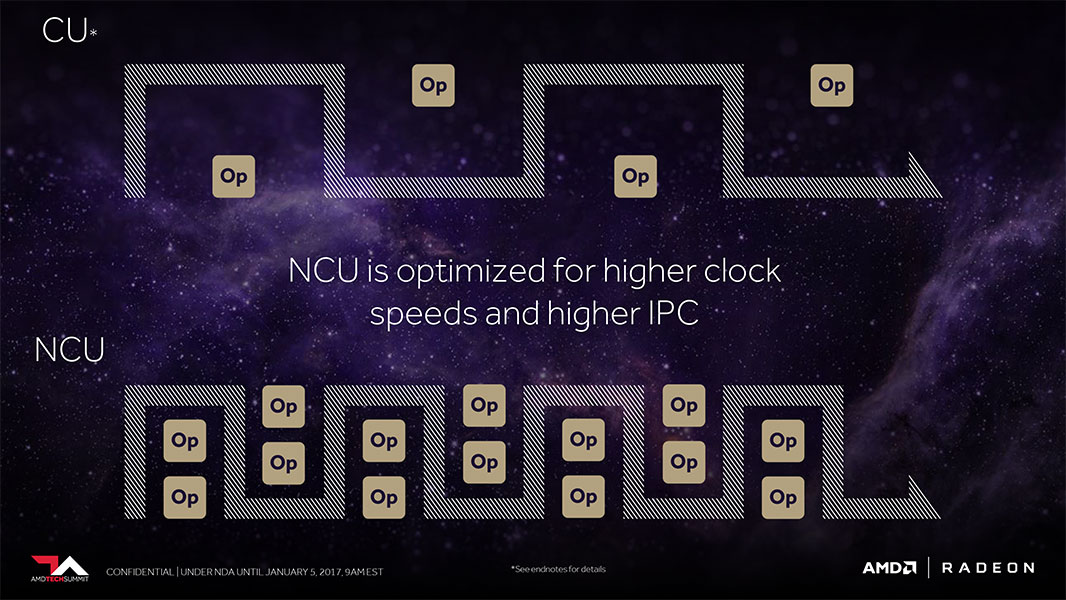
AMD also introduced a new feature called "Rapid Packed Math" in which it clumps multiple 16-bit operations between 32-bit registers for more simple work done per clock. Thanks to these improvements, the Vega NCU is able to crunch four times the operations per clock cycle as the previous generation, as well as run at double the clock speed. AMD has carried over its memory bandwidth-saving lossless compression algorithms. Lastly, AMD improved the pixel-engine with a new-generation draw-stream binning rasterizer. This conserves clock cycles, which helps with on-die cache locality and memory footprint.
AMD changed the hierarchy of the GPU in a way that improves performance of apps that use deferred shading. The geometry pipeline, the compute engine, and and the pixel engine, which output to the ROPs (L1 caches), are now tied to the L2 cache. Earlier, the pixel and texture engines had non-coherent memory access in which the pixel engine wrote to the memory controller.
Our Patreon Silver Supporters can read articles in single-page format.
Apr 25th, 2024 09:30 EDT
change timezone
Latest GPU Drivers
New Forum Posts
- Asrock A770 Firmware (1)
- RTX 4070 vs RTX 4070 Ti power scaling (5)
- i7-12800HX Overheating Issues (2)
- (Anti) SFF fun house (354)
- What's your latest tech purchase? (20339)
- Alphacool CORE 1 CPU block - bulging with danger of splitting? (6)
- Bizarre Throttlestop issue (6)
- Core i5-6300U (17)
- Last game you purchased? (255)
- Drop fps (4)
Popular Reviews
- Fractal Design Terra Review
- Thermalright Phantom Spirit 120 EVO Review
- Corsair 2000D Airflow Review
- Minisforum EliteMini UM780 XTX (AMD Ryzen 7 7840HS) Review
- ASUS GeForce RTX 4090 STRIX OC Review
- NVIDIA GeForce RTX 4090 Founders Edition Review - Impressive Performance
- ASUS GeForce RTX 4090 Matrix Platinum Review - The RTX 4090 Ti
- MSI GeForce RTX 4090 Suprim X Review
- MSI GeForce RTX 4090 Gaming X Trio Review
- Gigabyte GeForce RTX 4090 Gaming OC Review
Controversial News Posts
- Sony PlayStation 5 Pro Specifications Confirmed, Console Arrives Before Holidays (116)
- NVIDIA Points Intel Raptor Lake CPU Users to Get Help from Intel Amid System Instability Issues (106)
- AMD "Strix Halo" Zen 5 Mobile Processor Pictured: Chiplet-based, Uses 256-bit LPDDR5X (101)
- US Government Wants Nuclear Plants to Offload AI Data Center Expansion (98)
- Windows 11 Now Officially Adware as Microsoft Embeds Ads in the Start Menu (88)
- Developers of Outpost Infinity Siege Recommend Underclocking i9-13900K and i9-14900K for Stability on Machines with RTX 4090 (85)
- Windows 10 Security Updates to Cost $61 After 2025, $427 by 2028 (84)
- AMD's RDNA 4 GPUs Could Stick with 18 Gbps GDDR6 Memory (82)