 553
553
AMD Radeon VII 16 GB Review
Test Setup »High-resolution PCB Pictures
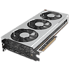
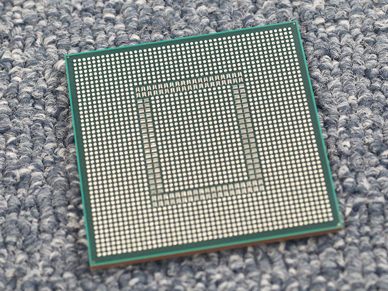
These pictures are for the convenience of volt-modders and those who would like to see all the finer details on the PCB. Feel free to link back to us and use them in your articles or forum posts.
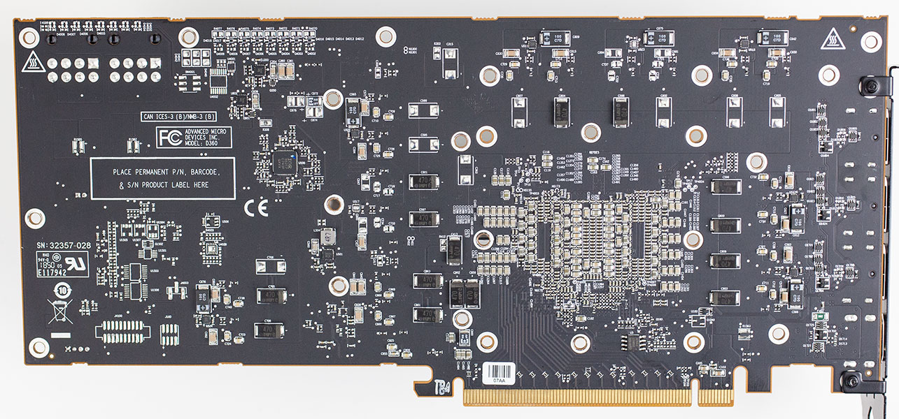
High-res versions are also available (front, back).
Circuit Board (PCB) Analysis

The GPU VRM is 10-phase, controlled by an International Rectifier IR35217 controller, which is among the best controllers available on the market. Do note the two empty solder pads for additional phases, which could be populated on AMD's Radeon Instinct MI60 with the full 4096 shaders of the chip active.


A second IR35217 is used to control two additional voltages, each with a two-phase design. I did check, and the four phases are not interconnected, which makes this a 10+2+2 VRM design.

Unlike the first-generation Vega 10, AMD has chosen to use four HBM2 memory stacks on Radeon VII, which doubles memory bus width to 4096 bit, while doubling total available memory bandwidth for over a terabyte per second as well! This design choice is also the reason why Radeon VII comes with 16 GB of memory instead of less, like 8 GB or 12 GB. At this time, only 4 GB and 8 GB HBM2 memory stacks exist; smaller or odd capacities are theoretically available through custom designs, but at much higher cost. Having four stacks is required to achieve the desired 4096 bit bus width, so the only memory size options are 16 GB and 32 GB. In theory, it could be possible to create a 3-stack 12 GB version with 25% lower memory bandwidth, resulting in a performance hit; another caveat is that we don't know if the Vega memory controller can even run with a non-power-of-two number of stacks. Our review sample uses Hynix HBM2 memory (H5VR32ESA4H-N0C)
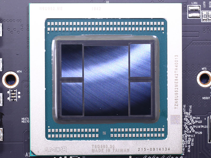
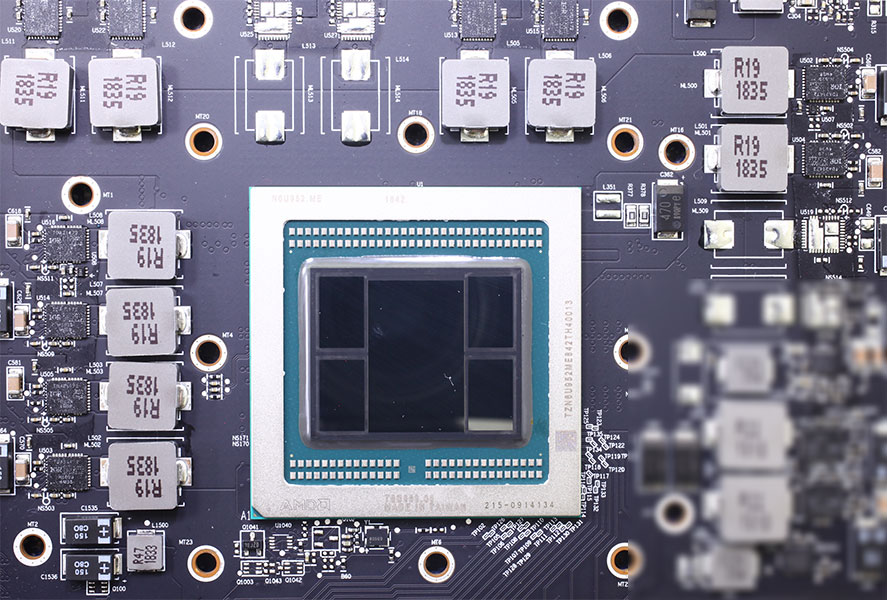
AMD's Vega 20 graphics processor is the first GPU in the world that's produced on a 7 nanometer production process. This not only reduces die size, but also enables higher clock frequencies with reduced power usage. Vega 20 is produced at TSMC Taiwan, using 13.2 billion transistors on a die size of 331 mm².
The pictured GPU chip actually consists of three different kinds of silicon. The large GPU chip you see in the middle, the four HBM2 memory stacks and, below both, covering the whole inner area, an interposer, which is a special chip design that only serves to connect the microscopic memory interface pins with their counterparts on the GPU die.
Apr 26th, 2024 20:45 EDT
change timezone
Latest GPU Drivers
New Forum Posts
- looking to build a new system and im considering asrock brand but i have some doubts/concerns. (15)
- AAF Optimus DCH Audio Modded Driver for Windows 10/11 - For ALL HDAUDIO Enumerator Chips (652)
- Help me identify rx 580 card ? (0)
- Strange system crashes out of nowhere help (9)
- What phone you use as your daily driver? And, a discussion of them. (1494)
- Secure boot already open help (11)
- TechPowerUp Screenshot Thread (MASSIVE 56K WARNING) (4213)
- The Official Linux/Unix Desktop Screenshots Megathread (705)
- Alphacool CORE 1 CPU block - bulging with danger of splitting? (32)
- Your PC ATM (34508)
Popular Reviews
- Ugreen NASync DXP4800 Plus Review
- MOONDROP x Crinacle DUSK In-Ear Monitors Review - The Last 5%
- HYTE THICC Q60 240 mm AIO Review
- CeBIT 2008: Cyber E Sport Review
- CeBIT 2008: Akasa Review
- Thermalright Phantom Spirit 120 EVO Review
- Alienware Pro Wireless Gaming Keyboard Review
- Upcoming Hardware Launches 2023 (Updated Feb 2024)
- Gigabyte Radeon RX 6700 XT Gaming OC Review
- Cougar GX-F Series 750W Review
Controversial News Posts
- Windows 11 Now Officially Adware as Microsoft Embeds Ads in the Start Menu (135)
- Sony PlayStation 5 Pro Specifications Confirmed, Console Arrives Before Holidays (117)
- NVIDIA Points Intel Raptor Lake CPU Users to Get Help from Intel Amid System Instability Issues (106)
- AMD "Strix Halo" Zen 5 Mobile Processor Pictured: Chiplet-based, Uses 256-bit LPDDR5X (103)
- US Government Wants Nuclear Plants to Offload AI Data Center Expansion (98)
- AMD's RDNA 4 GPUs Could Stick with 18 Gbps GDDR6 Memory (95)
- Developers of Outpost Infinity Siege Recommend Underclocking i9-13900K and i9-14900K for Stability on Machines with RTX 4090 (85)
- Windows 10 Security Updates to Cost $61 After 2025, $427 by 2028 (84)