 15
15
AMD Ryzen 3 3100 Review - Disruptive Price/Performance
(15 Comments) »Introduction
Here's the cheapest AMD processor based on its fastest 7 nm "Zen 2" architecture, the Ryzen 3 3100. This is a chip of many firsts. It is the first to bring 4-cores and 8-threads under the $100-mark, the first with PCI-Express gen 4.0 in this segment, and one of the first with an unlocked multiplier (a distinction held by its compatriot, the Athlon 3000G). What's more surprising is that AMD did not disable any of its I/O features. You get the same I/O goodies as the $750 Ryzen 9 3950X! At its price of just $99, the Ryzen 3 3100 in this review goes right up against several Intel 9th Gen Core i3 and 10th Gen Pentium SKUs.
The Ryzen 3 3100 and Ryzen 3 3300X launching today are based on the same single-chiplet "Matisse" MCM as the rest of the 3rd generation Ryzen desktop processor series. This 4-core/8-thread processor ticks at 3.60 GHz with 3.90 GHz boost frequency, and supports the same high-frequency DDR4 memory modules as the rest of the series. You also get future-proofing in the form of PCI-Express gen 4.0, which you can use with motherboards based on the new B550 chipset or the premium X570 chipset. With a BIOS update, the processor is also compatible with older motherboards based on AMD 400-series chipsets.
AMD carved out the Ryzen 3 3100 by taking a single-chiplet "Matisse" processor, similar to a Ryzen 7 3800X, disabling two cores per CCX, and halving the L3 cache on both. It hence ends up as a quad-core part with a 2+2 CCX configuration. Each of the two cores per CCX has access to up to 8 MB of L3 cache. With 512 KB L2 cache per core and 16 MB of L3 cache, the caches add up to 18 MB "total cache." The Ryzen 3 3300X takes a slightly different approach, which you can read about in its review.
With prices of just $99 for the 3100 and $120 for the 3300X, AMD is hoping to woo the mainstream gaming crowd by letting them allocate more of their PC building budget to the graphics card. You'll need one, as unlike the Ryzen 3 3200G "Picasso," the Ryzen 3100 and 3300X lack integrated graphics. The processor's TDP is rated at 65 W.
We review the Ryzen 3 3100 in this article, comparing it with a broad spectrum of processors across our refreshed CPU bench.
| Price | Cores / Threads | Base Clock | Max. Boost | L3 Cache | TDP | Architecture | Process | Socket | |
|---|---|---|---|---|---|---|---|---|---|
| Athlon 3000G | $50 | 2 / 4 | 3.5 GHz | N/A | 4 MB | 35 W | Zen | 14 nm | AM4 |
| Athlon 200GE | $55 | 2 / 4 | 3.2 GHz | N/A | 4 MB | 35 W | Zen | 14 nm | AM4 |
| Ryzen 3 1200 | $60 | 4 / 4 | 3.1 GHz | 3.4 GHz | 8 MB | 65 W | Zen | 14 nm | AM4 |
| Core i3-9100F | $75 | 4 / 4 | 3.6 GHz | 4.2 GHz | 6 MB | 65 W | Coffee Lake | 14 nm | LGA 1151 |
| Athlon 240GE | $80 | 2 / 4 | 3.5 GHz | N/A | 4 MB | 35 W | Zen | 14 nm | AM4 |
| Ryzen 3 2200G | $85 | 4 / 4 | 3.5 GHz | 3.7 GHz | 4 MB | 65 W | Zen | 14 nm | AM4 |
| Ryzen 3 3100 | $100 | 4 / 8 | 3.6 GHz | 3.9 GHz | 16 MB | 65 W | Zen 2 | 7 nm | AM4 |
| Pentium G5600 | $100 | 2 / 4 | 3.9 GHz | N/A | 4 MB | 54 W | Coffee Lake | 14 nm | LGA 1151 |
| Ryzen 5 1400 | $105 | 4 / 8 | 3.2 GHz | 3.4 GHz | 8 MB | 65 W | Zen | 14 nm | AM4 |
| Ryzen 3 1300X | $115 | 4 / 4 | 3.4 GHz | 3.7 GHz | 8 MB | 65 W | Zen | 14 nm | AM4 |
| Ryzen 5 1600 | $110 | 6 / 12 | 3.2 GHz | 3.6 GHz | 16 MB | 65 W | Zen | 14 nm | AM4 |
| Ryzen 3 3300X | $120 | 4 / 8 | 3.8 GHz | 4.3 GHz | 16 MB | 65 W | Zen 2 | 7 nm | AM4 |
| Ryzen 5 2600 | $120 | 6 / 12 | 3.4 GHz | 3.9 GHz | 16 MB | 65 W | Zen | 12 nm | AM4 |
| Core i3-8300 | $140 | 4 / 4 | 3.7 GHz | N/A | 8 MB | 65 W | Coffee Lake | 14 nm | LGA 1151 |
| Ryzen 5 1500X | $140 | 4 / 8 | 3.5 GHz | 3.7 GHz | 16 MB | 65 W | Zen | 14 nm | AM4 |
| Ryzen 5 2400G | $150 | 4 / 8 | 3.6 GHz | 3.9 GHz | 4 MB | 65 W | Zen | 14 nm | AM4 |
| Ryzen 5 1600X | $150 | 6 / 12 | 3.6 GHz | 4.0 GHz | 16 MB | 95 W | Zen | 14 nm | AM4 |
| Ryzen 5 2600X | $150 | 6 / 12 | 3.6 GHz | 4.2 GHz | 16 MB | 95 W | Zen | 12 nm | AM4 |
| Core i5-9400F | $160 | 6 / 6 | 2.9 GHz | 4.1 GHz | 9 MB | 65 W | Coffee Lake | 14 nm | LGA 1151 |
| Ryzen 7 1700 | $170 | 8 / 16 | 3.0 GHz | 3.7 GHz | 16 MB | 65 W | Zen | 14 nm | AM4 |
| Ryzen 7 1700X | $170 | 8 / 16 | 3.4 GHz | 3.8 GHz | 16 MB | 95 W | Zen | 14 nm | AM4 |
| Ryzen 5 3600 | $175 | 6 / 12 | 3.8 GHz | 4.4 GHz | 32 MB | 65 W | Zen 2 | 7 nm | AM4 |
| Ryzen 7 2700 | $170 | 8 / 16 | 3.2 GHz | 4.1 GHz | 16 MB | 65 W | Zen | 12 nm | AM4 |
| Core i5-8400 | $190 | 6 / 6 | 2.8 GHz | 4.0 GHz | 9 MB | 65 W | Coffee Lake | 14 nm | LGA 1151 |
| Ryzen 7 2700X | $195 | 8 / 16 | 3.7 GHz | 4.3 GHz | 16 MB | 105 W | Zen | 12 nm | AM4 |
| Core i3-8350K | $195 | 4 / 4 | 4.0 GHz | N/A | 8 MB | 91 W | Coffee Lake | 14 nm | LGA 1151 |
| Core i5-8600K | $250 | 6 / 6 | 3.6 GHz | 4.3 GHz | 9 MB | 95 W | Coffee Lake | 14 nm | LGA 1151 |
| Core i5-9600K | $200 | 6 / 6 | 3.7 GHz | 4.6 GHz | 9 MB | 95 W | Coffee Lake | 14 nm | LGA 1151 |
| Ryzen 5 3600X | $205 | 6 / 12 | 3.8 GHz | 4.4 GHz | 32 MB | 95 W | Zen 2 | 7 nm | AM4 |
A Closer Look
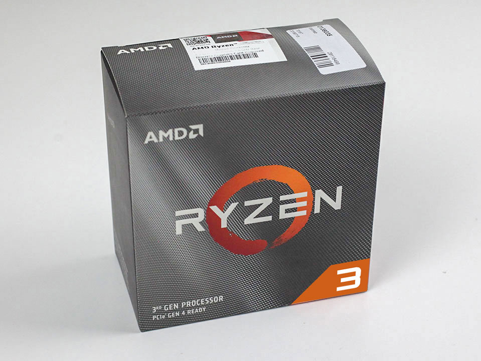
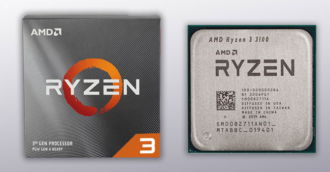
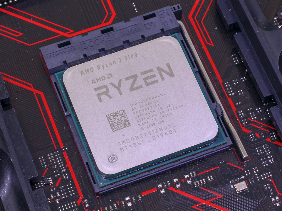
The Ryzen 3 3100 ships in a simple paperboard box with a window that shows the processor inside. The Ryzen motif of the carbon fiber pattern backdrop hints at this being a 3rd generation Ryzen chip.
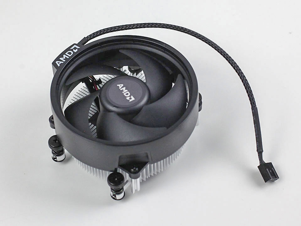

AMD includes a Wraith Stealth cooling solution with the Ryzen 3 3100. This is a noise-optimized cooler designed for chips with 65 W TDP.


The Ryzen 3 3100 processor looks like any conventional AMD processor with a large IHS dominating the top, and a 1,331-pin micro-PGA in the bottom. The "Zen 2" CCD chiplet is made in Taiwan, the I/O die in the US, and the two are put together at a facility in China.
The Ryzen 3 3100 can be paired with a fairly big selection of AM4-compatible coolers that have been released since 2017.
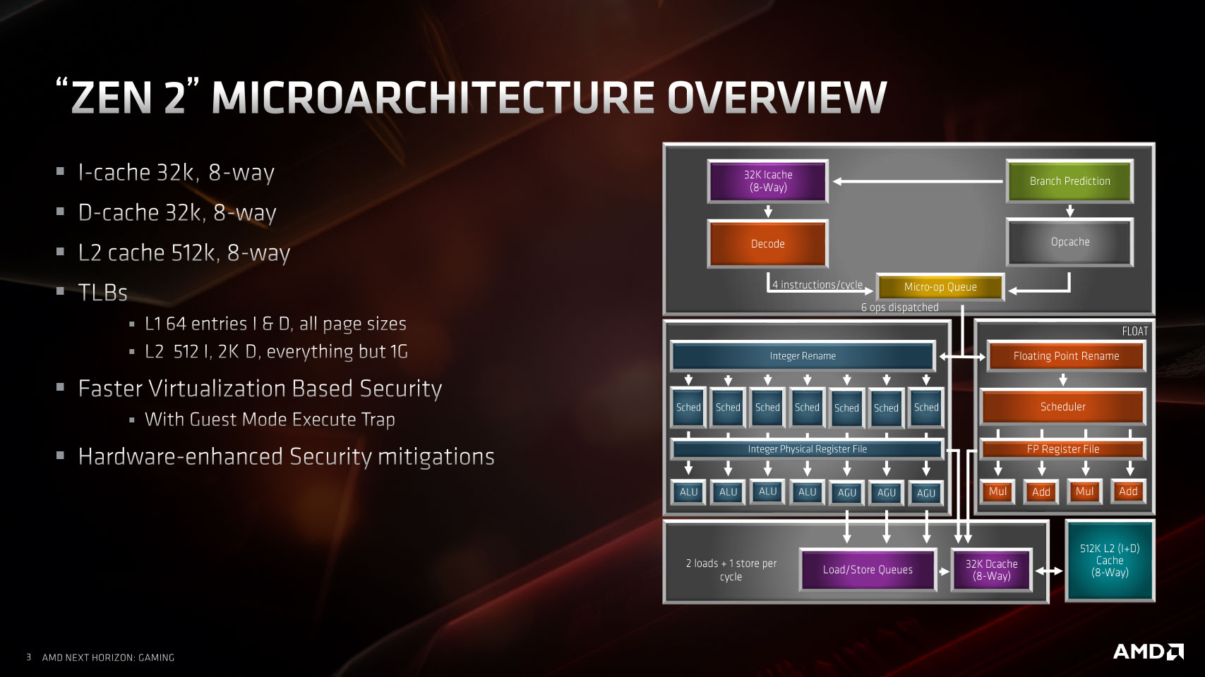
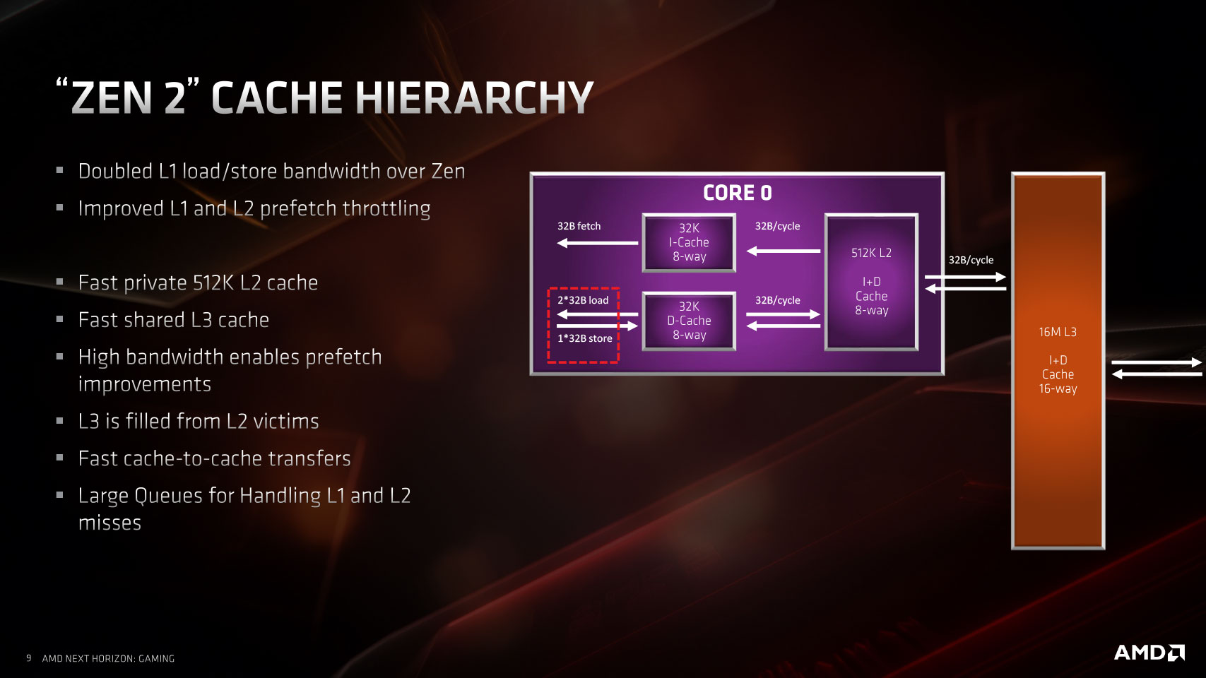
Architecture
The architecture is no different from the Ryzen 9 3950X or any other "Matisse," so you can click on the button below to read about it, or skip that section if you're familiar with it.


Architectural Innovations Specific to Ryzen 3 3300X and 3100
Both the Ryzen 3 3300X and Ryzen 3 3100 are 4-core/8-thread parts, but their segmentation goes beyond clock speeds to justify the 20% price gap between them. AMD tapped into the multi-core topology of its "Zen 2" microarchitecture to obtain the 4-core configuration differently between the two SKUs. Each 7 nm "Zen 2" chiplet (CCD) physically features eight CPU cores spread across two CCX (compute complexes) with four cores and 16 MB of L3 cache, each. For the 8-core Ryzen 7 parts, all eight cores are enabled. For the 6-core Ryzen 5 and 12-core dual-chiplet Ryzen 9 3900X, one core per CCX is disabled, yielding a 3+3 core CCX configuration.
The Ryzen 3 3300X and 3100 are designed differently at the CCX-level. For the entry-level 3100, AMD disabled two cores per CCX and reduced the L3 cache amount to 8 MB per CCX. This 2+2 core CCX configuration with 16 MB of L3 cache (2x 8 MB) still qualifies AMD's specs sheet. The 3300X has a key difference. One of the two CCX on the chiplet is completely disabled, and all four cores are localized to a single CCX, with its full 16 MB L3 cache enabled and shared between all four cores. This improves inter-core latency and lets a core access >8 MB of L3 cache if it wants. For the Ryzen 3 3100, inter-core communication between CCXs comes with certain performance costs arising from latency.
AMD B550 Chipset
With premium AMD X570 chipset-based motherboards starting at $150, it's less likely that someone would pair the 3rd gen Ryzen 3 with it. Choosing a cheaper B450 motherboard would mean giving up on killer features such as PCIe gen 4.0. AMD hence launched the new B550 mid-range chipset alongside these processors. Motherboards based on the new chipset are expected to be available around mid June, 2020, at starting prices similar to B450-based ones. The B550 chipset lets you have PCI-Express gen 4.0 connectivity from the "Matisse" processor, while limiting general purpose PCIe downstream connectivity to gen 3.0.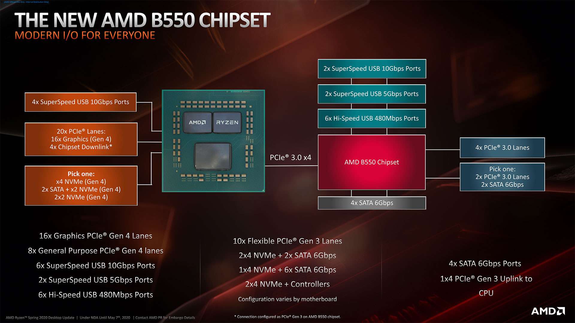
On a typical B550 chipset motherboard, the main PCI-Express x16 slot will be gen 4.0 if paired with a 3rd gen Ryzen "Matisse" processor, as would one of the board's M.2 NVMe slots that's wired to the processor. All other PCIe or M.2 slots which are wired to the B550 chipset will be gen 3.0. This way, future-proofing of the platform for next-generation graphics cards and SSDs remains intact. The B550 chipset provides up to six SATA 6 Gbps ports with AHCI and RAID capability, up to two 10 Gbps USB 3.1 gen 2 ports (in addition to four such ports put out by the "Matisse" processor), two additional USB 3.1 gen 1 ports, and six USB 2.0 ports. The platform's HDA and LPCIO buses are located on the processor.
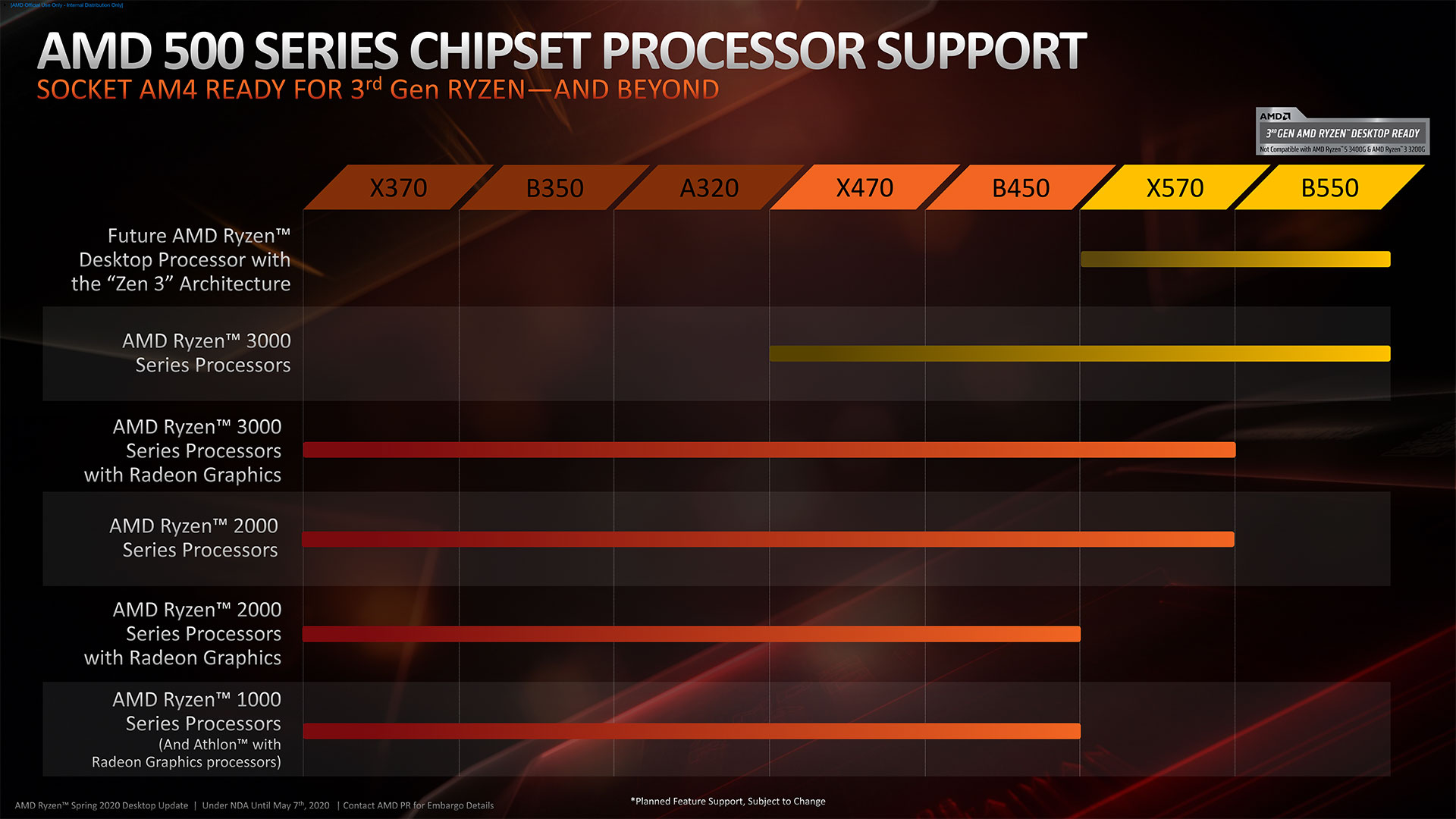
A word on compatibility: the B550 chipset only supports 3rd gen Ryzen "Matisse" processors as of this writing and AMD confirmed support for next-generation processors based on the "Zen 3" architecture. You cannot pair a B550 motherboard with older Ryzen 2000/1000 processors or even the 3200G or 3400G APUs based on the older "Zen+" microarchitecture. There will be clear labeling on B550 chipset motherboard boxes to this effect.
What we like most about the B550 is its low TDP, which lets motherboard designers make do with passive heatsinks; unlike X570, which requires active fan-heatsinks.
Our Patreon Silver Supporters can read articles in single-page format.
Apr 25th, 2024 00:20 EDT
change timezone
Latest GPU Drivers
New Forum Posts
- What's your latest tech purchase? (20337)
- The Official Linux/Unix Desktop Screenshots Megathread (694)
- XFX RX470 8GB no video and error 43 (27)
- (Anti) SFF fun house (348)
- Cinebench crashed my PC. My Wi-Fi stopped working, and I keep getting a "Please wait" screen when I boot up my PC. (31)
- im new to throttelstop and i think i messed it up by copying others any hints would be very much aprreciated (1)
- Aida64 cache mem OC (7)
- I am getting artifacting when I change Windows security settings. Is my GPU failing, or is this just a Windows issue? (10)
- Is there a technical reason that Windows 11 doesn't have built into it battery charge limitation? (42)
- The TPU UK Clubhouse (24783)
Popular Reviews
- Fractal Design Terra Review
- Thermalright Phantom Spirit 120 EVO Review
- Corsair 2000D Airflow Review
- Minisforum EliteMini UM780 XTX (AMD Ryzen 7 7840HS) Review
- ASUS GeForce RTX 4090 STRIX OC Review
- NVIDIA GeForce RTX 4090 Founders Edition Review - Impressive Performance
- ASUS GeForce RTX 4090 Matrix Platinum Review - The RTX 4090 Ti
- MSI GeForce RTX 4090 Suprim X Review
- MSI GeForce RTX 4090 Gaming X Trio Review
- Gigabyte GeForce RTX 4090 Gaming OC Review
Controversial News Posts
- Sony PlayStation 5 Pro Specifications Confirmed, Console Arrives Before Holidays (116)
- NVIDIA Points Intel Raptor Lake CPU Users to Get Help from Intel Amid System Instability Issues (106)
- AMD "Strix Halo" Zen 5 Mobile Processor Pictured: Chiplet-based, Uses 256-bit LPDDR5X (101)
- US Government Wants Nuclear Plants to Offload AI Data Center Expansion (98)
- Windows 10 Security Updates to Cost $61 After 2025, $427 by 2028 (84)
- Developers of Outpost Infinity Siege Recommend Underclocking i9-13900K and i9-14900K for Stability on Machines with RTX 4090 (84)
- TechPowerUp Hiring: Reviewers Wanted for Motherboards, Laptops, Gaming Handhelds and Prebuilt Desktops (78)
- AMD's RDNA 4 GPUs Could Stick with 18 Gbps GDDR6 Memory (73)