 115
115
AMD Ryzen 3 3300X Review - The Magic of One CCX
(115 Comments) »Introduction
AMD today announced its 3rd generation Ryzen 3 desktop processor family based on the 7 nm "Zen 2" microarchitecture designed to compete with Intel's 10th generation Core i3 desktop processors at highly competitive price points. These include the Ryzen 3 3300X we're reviewing here and the entry-level Ryzen 3 3100, which is today's second review. This series is not to be confused with the Ryzen 3 3200G, which is a 12 nm APU based on the "Picasso" silicon and the "Zen+" microarchitecture. Both the 3300X and 3100 are 4-core/8-thread parts and see the introduction of SMT to the Ryzen 3 brand.
The Ryzen 3 3300X is based on the same "Matisse" multi-chip module design as the rest of the 3rd gen Ryzen processor family. While the higher-end models above the Ryzen 7 3800X use two chipsets, Ryzen 3 3300X uses a single 7 nm "Zen 2" chiplet paired with the same exact I/O die as the rest of the family. What this means is that the 3300X and 3100 offer the same I/O feature set as the $750 Ryzen 9 3950X.

AMD's Ryzen 3 3300X introduces segment-first PCI-Express gen 4.0 support. When paired with an AMD B550 or X570 chipset motherboard, these chips offer a PCI-Express 4.0 x16 port for graphics, at least one M.2 NVMe slot with fast PCI-Express 4.0 x4 wiring, and support for significantly faster DDR4 memory standards than previous generations of Ryzen. These chips are practically as feature-rich as a Ryzen 5 3600 or 3700X, or 3950X, but with four cores (and eight threads).
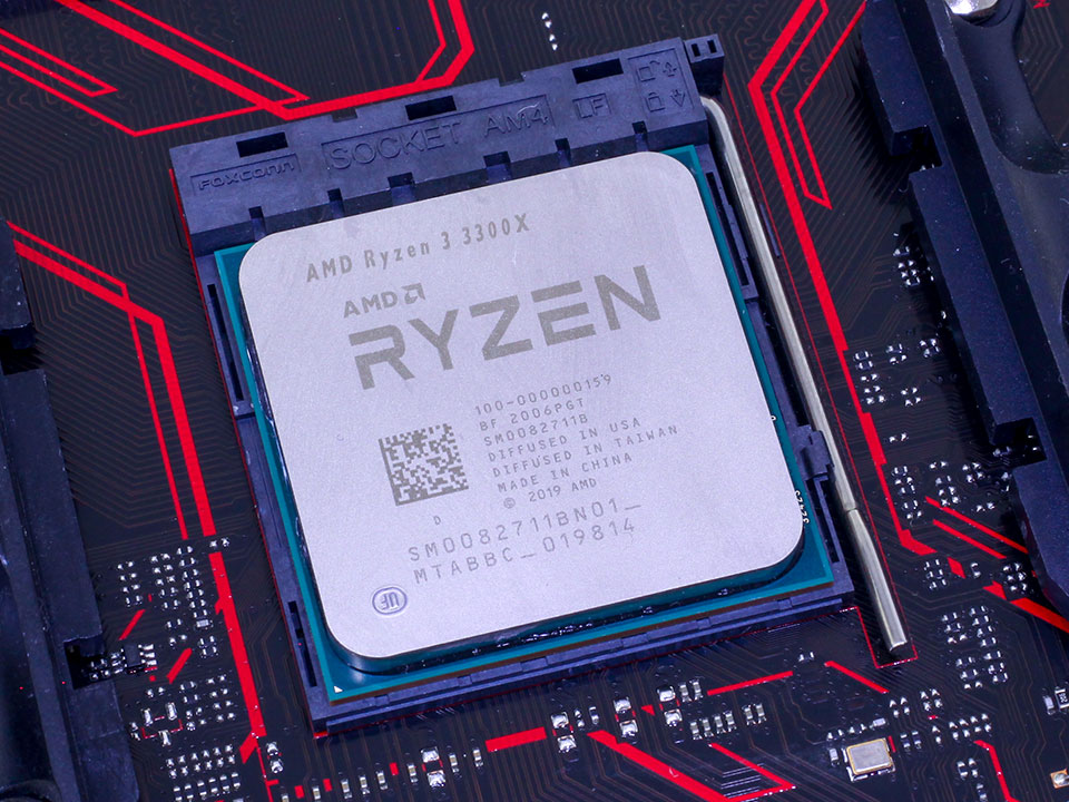
The processor in this Ryzen 3 3300X review is clocked at 3.80 GHz nominal and has a max boost frequency of 4.30 GHz, as well as an unlocked multiplier that lets you overclock it further. Its four "Zen 2" CPU cores are localized to a single CCX inside a 7 nm chiplet (CCD), and it hence has a cache hierarchy of 512 KB L2 cache per core, and 16 MB of L3 cache uniformly shared between all four cores. This takes the "total cache" count, as AMD likes to call it, to 18 MB. The processor's TDP is rated at 65 W.
AMD is surprising both buyers and its competition with pricing. The 3300X is priced at just $120, a price at which Intel's cheapest Core i3-10100 starts. The Ryzen 3 3100 is even cheaper at just $100. At these prices, AMD is giving you unlocked multipliers for effortless overclocking and the in-box Wraith Stealth cooling solution. The TDP of both chips is rated at 65 W. The processor is compatible with AMD X570, B550, and older 400-series chipsets for which BIOS updates are needed.
In this review, we take the Ryzen 3 3300X for a spin across our refreshed CPU bench, where we pit it against a broad spectrum of rivals.
| Price | Cores / Threads | Base Clock | Max. Boost | L3 Cache | TDP | Architecture | Process | Socket | |
|---|---|---|---|---|---|---|---|---|---|
| Athlon 3000G | $50 | 2 / 4 | 3.5 GHz | N/A | 4 MB | 35 W | Zen | 14 nm | AM4 |
| Athlon 200GE | $55 | 2 / 4 | 3.2 GHz | N/A | 4 MB | 35 W | Zen | 14 nm | AM4 |
| Ryzen 3 1200 | $60 | 4 / 4 | 3.1 GHz | 3.4 GHz | 8 MB | 65 W | Zen | 14 nm | AM4 |
| Core i3-9100F | $75 | 4 / 4 | 3.6 GHz | 4.2 GHz | 6 MB | 65 W | Coffee Lake | 14 nm | LGA 1151 |
| Athlon 240GE | $80 | 2 / 4 | 3.5 GHz | N/A | 4 MB | 35 W | Zen | 14 nm | AM4 |
| Ryzen 3 2200G | $85 | 4 / 4 | 3.5 GHz | 3.7 GHz | 4 MB | 65 W | Zen | 14 nm | AM4 |
| Ryzen 3 3100 | $100 | 4 / 8 | 3.6 GHz | 3.9 GHz | 16 MB | 65 W | Zen 2 | 7 nm | AM4 |
| Pentium G5600 | $100 | 2 / 4 | 3.9 GHz | N/A | 4 MB | 54 W | Coffee Lake | 14 nm | LGA 1151 |
| Ryzen 5 1400 | $105 | 4 / 8 | 3.2 GHz | 3.4 GHz | 8 MB | 65 W | Zen | 14 nm | AM4 |
| Ryzen 3 1300X | $115 | 4 / 4 | 3.4 GHz | 3.7 GHz | 8 MB | 65 W | Zen | 14 nm | AM4 |
| Ryzen 5 1600 | $110 | 6 / 12 | 3.2 GHz | 3.6 GHz | 16 MB | 65 W | Zen | 14 nm | AM4 |
| Ryzen 3 3300X | $120 | 4 / 8 | 3.8 GHz | 4.3 GHz | 16 MB | 65 W | Zen 2 | 7 nm | AM4 |
| Ryzen 5 2600 | $120 | 6 / 12 | 3.4 GHz | 3.9 GHz | 16 MB | 65 W | Zen | 12 nm | AM4 |
| Core i3-8300 | $140 | 4 / 4 | 3.7 GHz | N/A | 8 MB | 65 W | Coffee Lake | 14 nm | LGA 1151 |
| Ryzen 5 1500X | $140 | 4 / 8 | 3.5 GHz | 3.7 GHz | 16 MB | 65 W | Zen | 14 nm | AM4 |
| Ryzen 5 2400G | $150 | 4 / 8 | 3.6 GHz | 3.9 GHz | 4 MB | 65 W | Zen | 14 nm | AM4 |
| Ryzen 5 1600X | $150 | 6 / 12 | 3.6 GHz | 4.0 GHz | 16 MB | 95 W | Zen | 14 nm | AM4 |
| Ryzen 5 2600X | $150 | 6 / 12 | 3.6 GHz | 4.2 GHz | 16 MB | 95 W | Zen | 12 nm | AM4 |
| Core i5-9400F | $160 | 6 / 6 | 2.9 GHz | 4.1 GHz | 9 MB | 65 W | Coffee Lake | 14 nm | LGA 1151 |
| Ryzen 7 1700 | $170 | 8 / 16 | 3.0 GHz | 3.7 GHz | 16 MB | 65 W | Zen | 14 nm | AM4 |
| Ryzen 7 1700X | $170 | 8 / 16 | 3.4 GHz | 3.8 GHz | 16 MB | 95 W | Zen | 14 nm | AM4 |
| Ryzen 5 3600 | $175 | 6 / 12 | 3.8 GHz | 4.4 GHz | 32 MB | 65 W | Zen 2 | 7 nm | AM4 |
| Ryzen 7 2700 | $170 | 8 / 16 | 3.2 GHz | 4.1 GHz | 16 MB | 65 W | Zen | 12 nm | AM4 |
| Core i5-8400 | $190 | 6 / 6 | 2.8 GHz | 4.0 GHz | 9 MB | 65 W | Coffee Lake | 14 nm | LGA 1151 |
| Ryzen 7 2700X | $195 | 8 / 16 | 3.7 GHz | 4.3 GHz | 16 MB | 105 W | Zen | 12 nm | AM4 |
| Core i3-8350K | $195 | 4 / 4 | 4.0 GHz | N/A | 8 MB | 91 W | Coffee Lake | 14 nm | LGA 1151 |
| Core i5-8600K | $250 | 6 / 6 | 3.6 GHz | 4.3 GHz | 9 MB | 95 W | Coffee Lake | 14 nm | LGA 1151 |
| Core i5-9600K | $200 | 6 / 6 | 3.7 GHz | 4.6 GHz | 9 MB | 95 W | Coffee Lake | 14 nm | LGA 1151 |
| Ryzen 5 3600X | $205 | 6 / 12 | 3.8 GHz | 4.4 GHz | 32 MB | 95 W | Zen 2 | 7 nm | AM4 |
A Closer Look
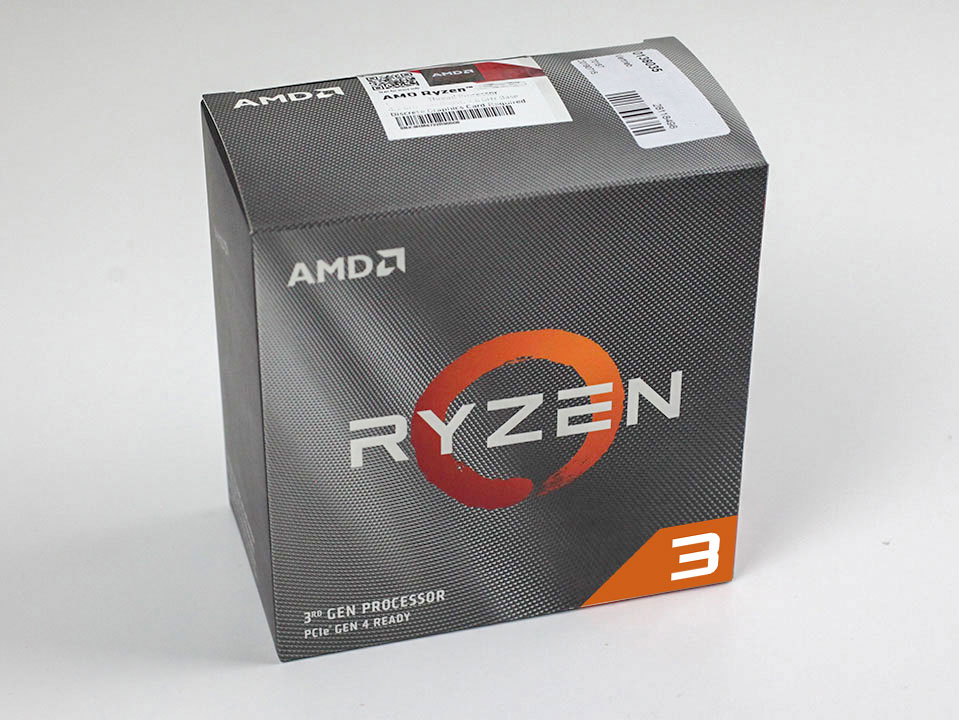
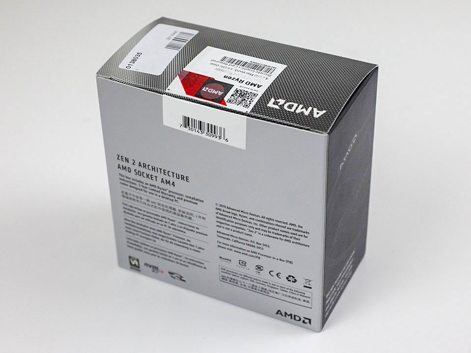
The Ryzen 3 3300X ships in a simple paperboard box with a window that shows the processor inside. The Ryzen motif in the carbon fiber pattern background hints at this being a 3rd generation Ryzen chip.
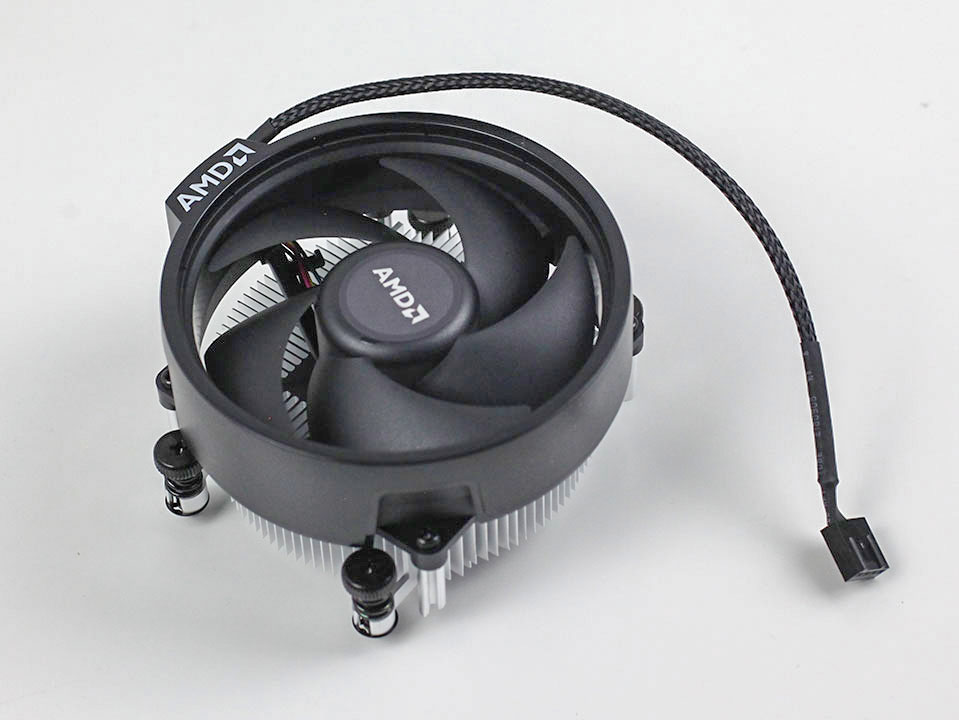
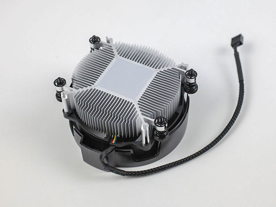
AMD includes a Wraith Stealth cooling solution with the Ryzen 3 3300X. This is a noise-optimized cooler designed for chips with 65 W TDP.


The Ryzen 3 3300X processor looks like any conventional AMD processor with a large IHS dominating the top, and a 1,331-pin micro-PGA in the bottom. The "Zen 2" CCD chiplet is made in Taiwan, the I/O die in the US, and the two are put together at a facility in China.
The Ryzen 3 3300X can be paired with a fairly big selection of AM4-compatible coolers that have been released since 2017.
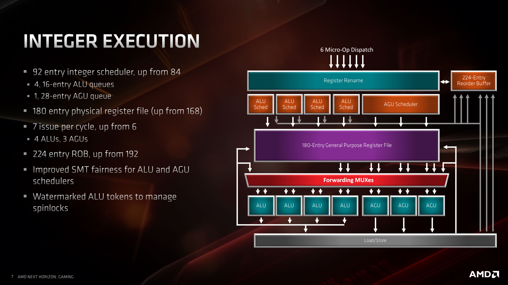
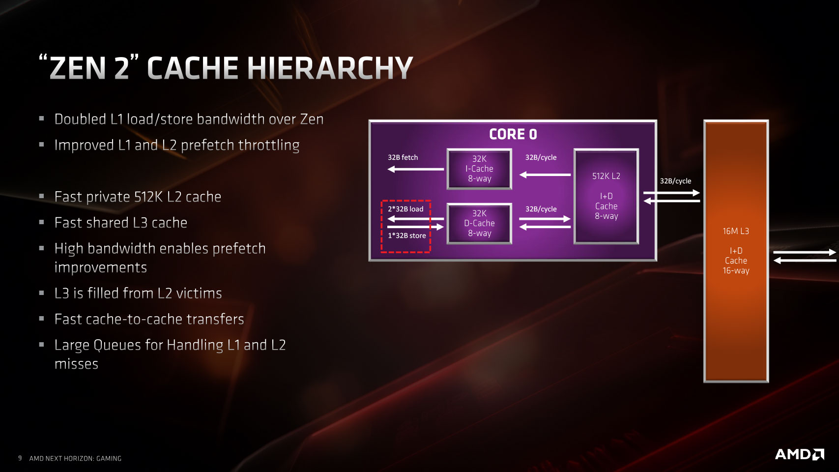
Architecture
The architecture is no different from the Ryzen 9 3950X or any other "Matisse," so you can click on the button below to read about it, or skip that section if you're familiar with it.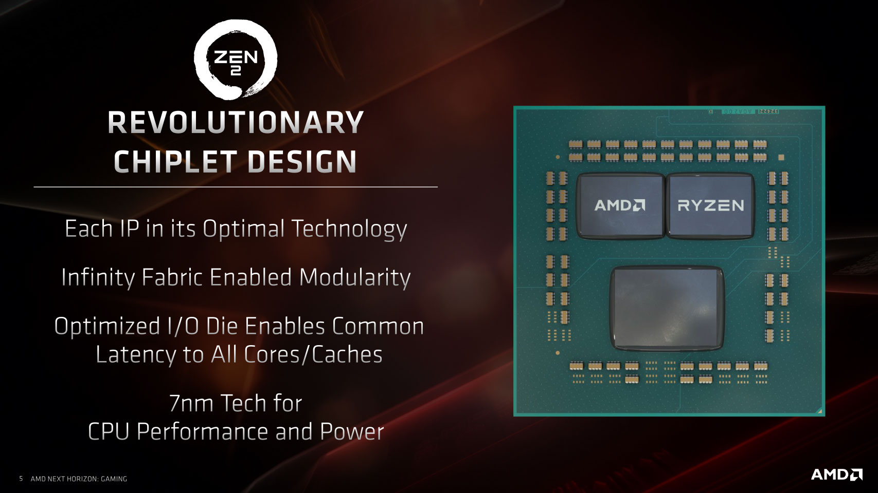


Architectural Innovations Specific to Ryzen 3 3300X and 3100
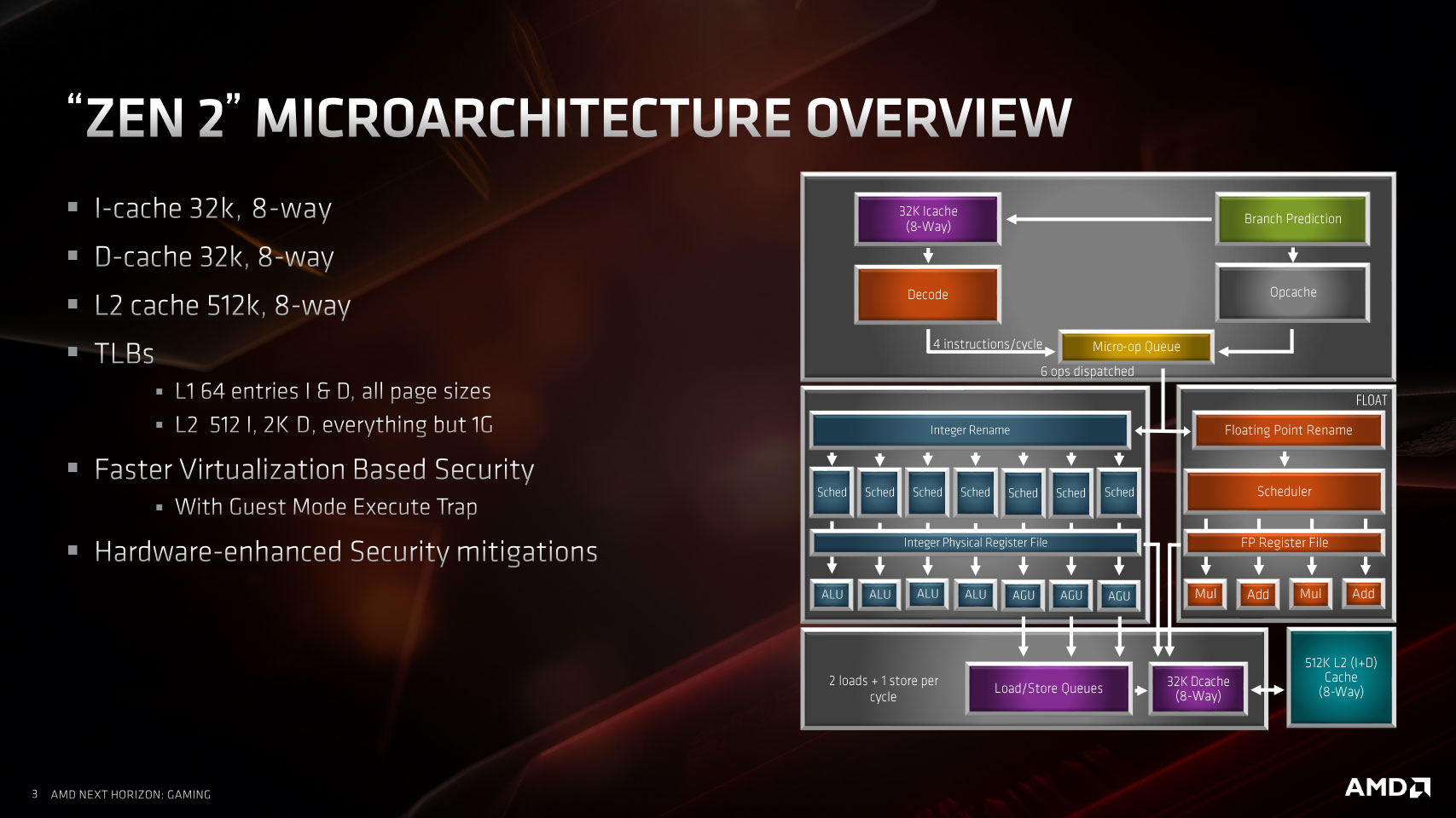
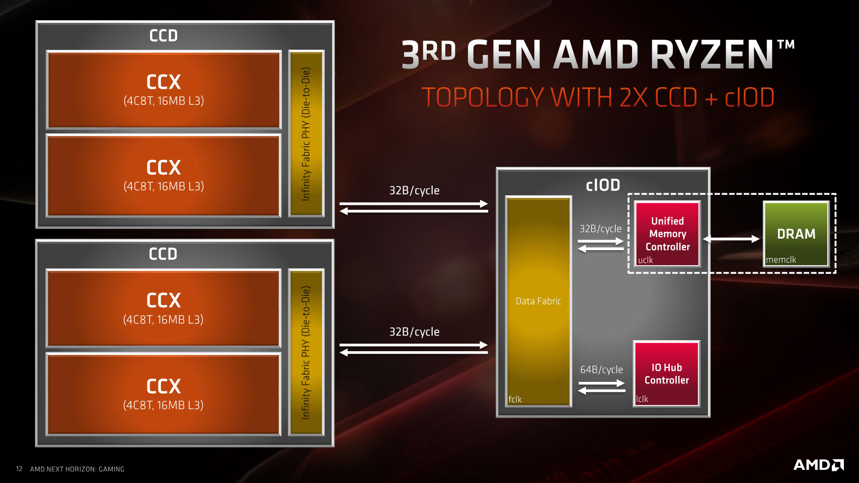
Both the Ryzen 3 3300X and Ryzen 3 3100 are 4-core/8-thread parts, but their segmentation goes beyond clock speeds to justify the 20% price gap between them. AMD tapped into the multi-core topology of its "Zen 2" microarchitecture to obtain the 4-core configuration differently between the two SKUs. Each 7 nm "Zen 2" chiplet (CCD) physically features eight CPU cores spread across two CCX (compute complexes) with four cores and 16 MB of L3 cache, each. For the 8-core Ryzen 7 parts, all eight cores are enabled. For the 6-core Ryzen 5 and 12-core dual-chiplet Ryzen 9 3900X, one core per CCX is disabled, yielding a 3+3 core CCX configuration.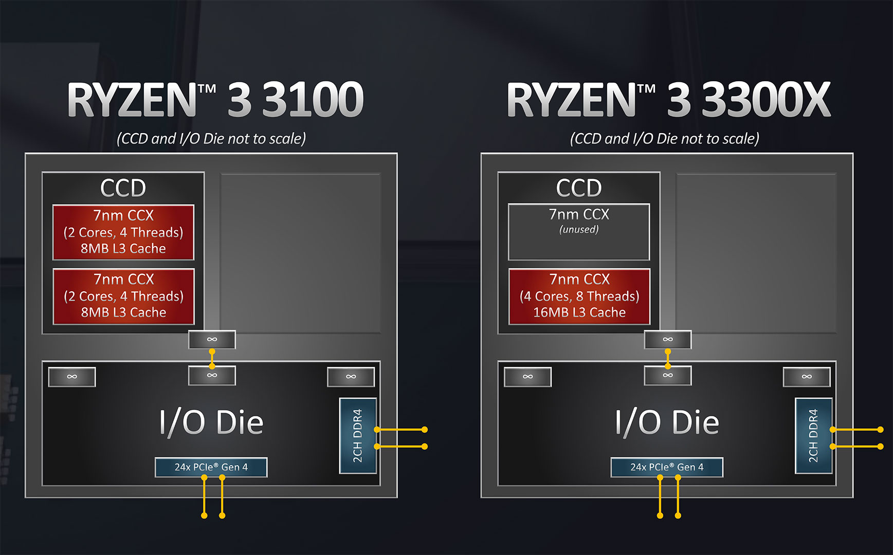
The Ryzen 3 3300X and 3100 are designed differently at the CCX-level. For the entry-level 3100, AMD disabled two cores per CCX and reduced the L3 cache amount to 8 MB per CCX. This 2+2 core CCX configuration with 16 MB of L3 cache (2x 8 MB) still qualifies AMD's specs sheet. The 3300X has a key difference. One of the two CCX on the chiplet is completely disabled, and all four cores are localized to a single CCX, with its full 16 MB L3 cache enabled and shared between all four cores. This improves inter-core latency and lets a core access >8 MB of L3 cache if it wants. For the Ryzen 3 3100, inter-core communication between CCXs comes with certain performance costs arising from latency.
AMD B550 Chipset
With premium AMD X570 chipset-based motherboards starting at $150, it's less likely that someone would pair the 3rd gen Ryzen 3 with it. Choosing a cheaper B450 motherboard would mean giving up on killer features such as PCIe gen 4.0. AMD hence launched the new B550 mid-range chipset alongside these processors. Motherboards based on the new chipset are expected to be available around mid June, 2020, at starting prices similar to B450-based ones. The B550 chipset lets you have PCI-Express gen 4.0 connectivity from the "Matisse" processor, while limiting general purpose PCIe downstream connectivity to gen 3.0.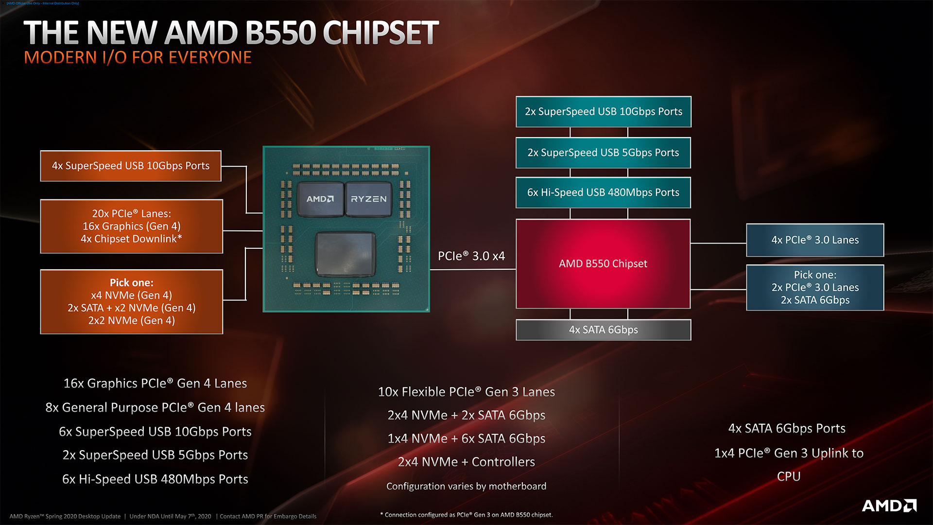
On a typical B550 chipset motherboard, the main PCI-Express x16 slot will be gen 4.0 if paired with a 3rd gen Ryzen "Matisse" processor, as would one of the board's M.2 NVMe slots that's wired to the processor. All other PCIe or M.2 slots which are wired to the B550 chipset will be gen 3.0. This way, future-proofing of the platform for next-generation graphics cards and SSDs remains intact. The B550 chipset provides up to six SATA 6 Gbps ports with AHCI and RAID capability, up to two 10 Gbps USB 3.1 gen 2 ports (in addition to the four such ports put out by the "Matisse" processor), two additional USB 3.1 gen 1 ports, and six USB 2.0 ports. The platform's HDA and LPCIO buses are located on the processor.
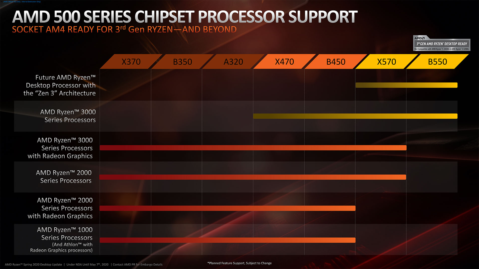
A word on compatibility. The B550 chipset only supports 3rd generation Ryzen "Matisse" processors as of this writing, and AMD confirmed support for next-generation processors based on the "Zen 3" architecture. You cannot pair a B550 motherboard with older Ryzen 2000/1000 processors or even the 3200G or 3400G APUs based on the older "Zen+" microarchitecture. There will be clear labeling on B550 chipset motherboard boxes to this effect.
What we like most about the B550 is its low TDP, which lets motherboard designers make do with passive heatsinks; unlike X570, which requires active fan heatsinks.
Our Patreon Silver Supporters can read articles in single-page format.
Apr 25th, 2024 23:38 EDT
change timezone
Latest GPU Drivers
New Forum Posts
- Alphacool CORE 1 CPU block - bulging with danger of splitting? (18)
- What's your latest tech purchase? (20340)
- Black screen after muting (5)
- What phone you use as your daily driver? And, a discussion of them. (1481)
- What are you playing? (20530)
- Secure boot already open help (0)
- TPU's Nostalgic Hardware Club (18465)
- Post your Speedometer 3.0 Score (36)
- Size on Disk Excessively Different than Size (9)
- Dell Workstation Owners Club (3056)
Popular Reviews
- Fractal Design Terra Review
- Thermalright Phantom Spirit 120 EVO Review
- Corsair 2000D Airflow Review
- ASUS GeForce RTX 4090 STRIX OC Review
- NVIDIA GeForce RTX 4090 Founders Edition Review - Impressive Performance
- ASUS GeForce RTX 4090 Matrix Platinum Review - The RTX 4090 Ti
- MSI GeForce RTX 4090 Suprim X Review
- Gigabyte GeForce RTX 4090 Gaming OC Review
- MSI GeForce RTX 4090 Gaming X Trio Review
- MSI GeForce RTX 4090 Suprim Liquid X Review
Controversial News Posts
- Sony PlayStation 5 Pro Specifications Confirmed, Console Arrives Before Holidays (117)
- Windows 11 Now Officially Adware as Microsoft Embeds Ads in the Start Menu (110)
- NVIDIA Points Intel Raptor Lake CPU Users to Get Help from Intel Amid System Instability Issues (106)
- AMD "Strix Halo" Zen 5 Mobile Processor Pictured: Chiplet-based, Uses 256-bit LPDDR5X (101)
- US Government Wants Nuclear Plants to Offload AI Data Center Expansion (98)
- AMD's RDNA 4 GPUs Could Stick with 18 Gbps GDDR6 Memory (88)
- Developers of Outpost Infinity Siege Recommend Underclocking i9-13900K and i9-14900K for Stability on Machines with RTX 4090 (85)
- Windows 10 Security Updates to Cost $61 After 2025, $427 by 2028 (84)