 34
34
AMD Ryzen 5 5600G Review - Affordable Zen 3 with Integrated Graphics
(34 Comments) »Introduction
AMD launched their Ryzen 5000G processors earlier this year for system integrators and OEMs—the DIY market had to wait a bit longer, until August. In our launch-day coverage, we brought you a review of the Ryzen 7 5700G. Today, we have the review of the Ryzen 5 5600G. The new processors are designed to fill important gaps in AMD's Ryzen 5000 series desktop processor lineup without stepping on or being stepped over by existing 5000X-series "Vermeer" desktop processors that lack integrated graphics. The 5000G series processors come with up to eight CPU cores based on the latest "Zen 3" microarchitecture, along with an integrated graphics solution based on "Vega," which has since been updated with display and codec improvements and dialed up in clock speeds.
At the heart of the Ryzen 7 5700G and Ryzen 5 5600G is the new 7 nm "Cezanne" silicon that made its debut with the company's Ryzen 5000 series mobile processors. This monolithic die features an 8-core/16-thread CPU, a Vega iGPU with up to eight compute units, updated display and media-engines, and the latest-generation memory. For the Ryzen 5 5600G in today's review, AMD has disabled two of the CPU cores, and set the IGP shader count to 448, down from 512 on the 5700G.

Besides the IPC uplift of the new Zen 3 CPU core, Cezanne benefits from the biggest design change of this generation, which is AMD effectively doing away with quad-core complexes and putting all eight cores into a single, large CCX with a common L3 cache. This significantly improves inter-core communication, handing over of threads between the cores, and multi-threaded performance in general. Also, since the CCX "partition" is done away with, the 8 Zen 3 cores share a single 16 MB L3 cache. This means the whole processor has only half the cache of Ryzen 5000X Vermeer, which offers 32 MB L3.
Unlike the other Zen 3 processors which feature PCIe 4.0, the Ryzen 5000G APUs come with a PCI-Express 3.0 interface. There's 16 lanes for the PCI-Express graphics slot, plus four for a CPU-connected M.2 NVMe slot, and four toward the chipset bus. Compared to older Ryzen APUs and even mobile Cezanne, this is still an improvement because those only had PCIe 3.0 x8 for external graphics. The other big change is optimizations to the dual-channel DDR4 memory controllers, which are capable of even higher memory frequencies.
Within AMD's product stack, AMD is positioning the Ryzen 7 5700G a notch below the Ryzen 7 5800X, and the Ryzen 5 5600G just below the Ryzen 5 5600X. The 5700G is filling in for the lack of a "Ryzen 7 5700X" (a successor to the popular Ryzen 7 3700X), while the 5600G has the equally important task of succeeding the immensely successful Ryzen 5 3600. AMD's sell here is that the monolithic design of the Cezanne silicon has some inherent advantages, such as lower latencies since the CPU cores, memory interface, and PCIe are sitting on the same die. Both chips do come with unlocked multipliers, so you can take a crack at overclocking them.
Priced at $260, the Ryzen 5 5600G is not cheap and sees strong competition from the Intel Core i5-11600K and AMD's own Ryzen 5 5600X.
| Price | Cores / Threads | Base Clock | Max. Boost | L3 Cache | TDP | Architecture | Process | Socket | |
|---|---|---|---|---|---|---|---|---|---|
| Ryzen 3 3300X | $240 | 4 / 8 | 3.8 GHz | 4.3 GHz | 16 MB | 65 W | Zen 2 | 7 nm | AM4 |
| Core i3-10300 | $180 | 4 / 8 | 3.7 GHz | 4.4 GHz | 8 MB | 65 W | Comet Lake | 14 nm | LGA 1200 |
| Core i5-9400F | $180 | 6 / 6 | 2.9 GHz | 4.1 GHz | 9 MB | 65 W | Coffee Lake | 14 nm | LGA 1151 |
| Core i5-10400F | $175 | 6 / 12 | 2.9 GHz | 4.3 GHz | 12 MB | 65 W | Comet Lake | 14 nm | LGA 1200 |
| Core i5-11400F | $240 | 6 / 12 | 2.6 GHz | 4.4 GHz | 12 MB | 65 W | Rocket Lake | 14 nm | LGA 1200 |
| Core i5-10500 | $270 | 6 / 12 | 3.1 GHz | 4.5 GHz | 12 MB | 65 W | Comet Lake | 14 nm | LGA 1200 |
| Ryzen 5 3600 | $280 | 6 / 12 | 3.6 GHz | 4.2 GHz | 32 MB | 65 W | Zen 2 | 7 nm | AM4 |
| Core i5-9600K | $215 | 6 / 6 | 3.7 GHz | 4.6 GHz | 9 MB | 95 W | Coffee Lake | 14 nm | LGA 1151 |
| Core i5-10600K | $270 | 6 / 12 | 4.1 GHz | 4.8 GHz | 12 MB | 125 W | Comet Lake | 14 nm | LGA 1200 |
| Core i5-11600K | $270 | 6 / 12 | 3.9 GHz | 4.9 GHz | 12 MB | 125 W | Rocket Lake | 14 nm | LGA 1200 |
| Ryzen 5 3600X | $290 | 6 / 12 | 3.8 GHz | 4.4 GHz | 32 MB | 95 W | Zen 2 | 7 nm | AM4 |
| Ryzen 5 5600G | $260 | 6 / 12 | 3.9 GHz | 4.4 GHz | 16 MB | 65 W | Zen 3 + Vega | 7 nm | AM4 |
| Ryzen 5 5600X | $300 | 6 / 12 | 3.7 GHz | 4.6 GHz | 32 MB | 65 W | Zen 3 | 7 nm | AM4 |
| Core i7-9700K | $290 | 8 / 8 | 3.6 GHz | 4.9 GHz | 12 MB | 95 W | Coffee Lake | 14 nm | LGA 1151 |
| Core i7-10700K | $330 | 8 / 16 | 3.8 GHz | 5.1 GHz | 16 MB | 125 W | Comet Lake | 14 nm | LGA 1200 |
| Core i7-11700K | $400 | 8 / 16 | 3.6 GHz | 5.0 GHz | 16 MB | 125 W | Rocket Lake | 14 nm | LGA 1200 |
| Ryzen 7 3700X | $315 | 8 / 16 | 3.6 GHz | 4.4 GHz | 32 MB | 65 W | Zen 2 | 7 nm | AM4 |
| Ryzen 7 5700G | $360 | 8 / 16 | 3.8 GHz | 4.6 GHz | 16 MB | 65 W | Zen 3 + Vega | 7 nm | AM4 |
| Ryzen 7 3800XT | $320 | 8 / 16 | 3.9 GHz | 4.7 GHz | 32 MB | 105 W | Zen 2 | 7 nm | AM4 |
| Ryzen 7 5800X | $400 | 8 / 16 | 3.8 GHz | 4.7 GHz | 32 MB | 105 W | Zen 3 | 7 nm | AM4 |
Unboxing and Photography
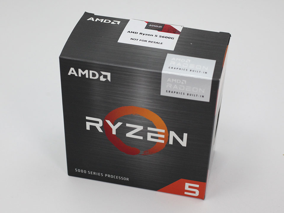
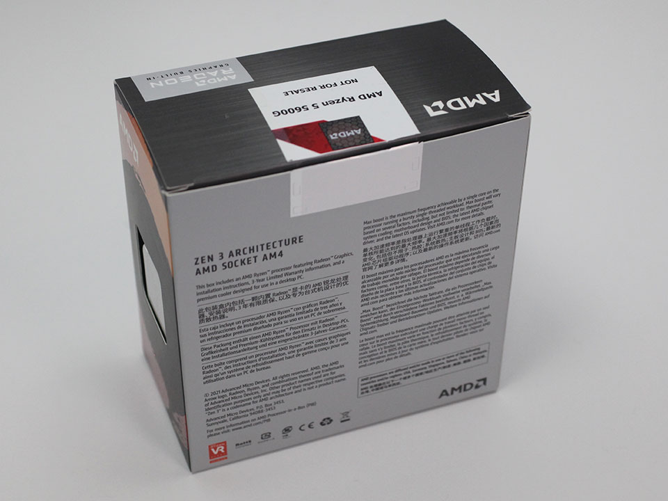
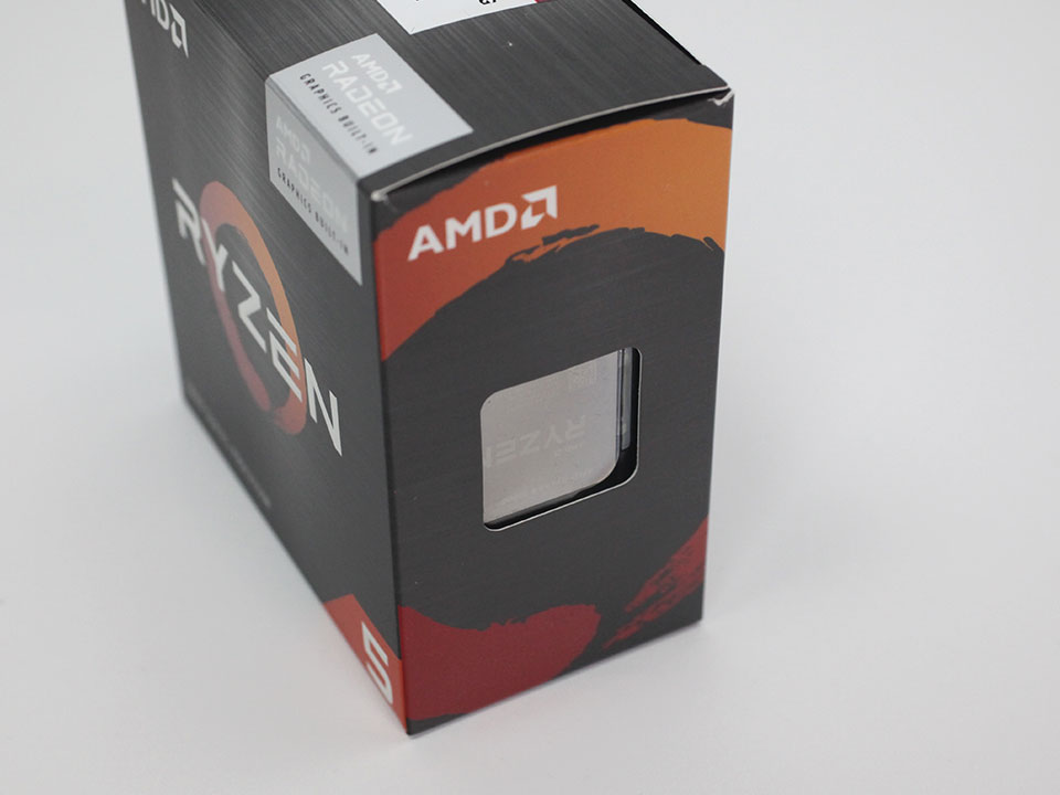
The Ryzen 5 5600G comes in a compact paperboard box featuring the same brushed metal look we saw on other Ryzen 5000 processors. The top-right of the package has a silvery note to clarify that this processor has integrated graphics. A small cutout on the side shows the actual processor inside the package.
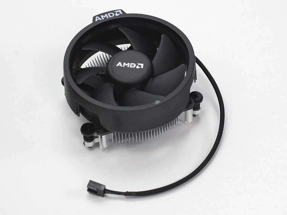
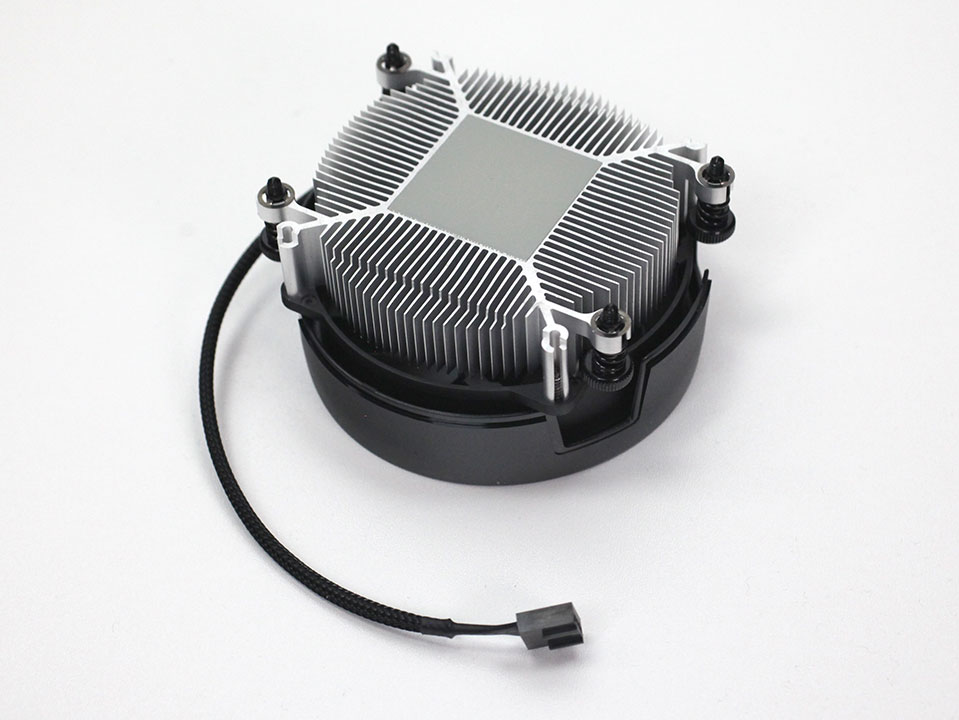
Unlike many other Zen 3 processors, the Ryzen 5 5600G includes a heatsink in the box. The Wraith Stealth cooling solution is suitable for the 65 W TDP of the Ryzen 5 5600G.
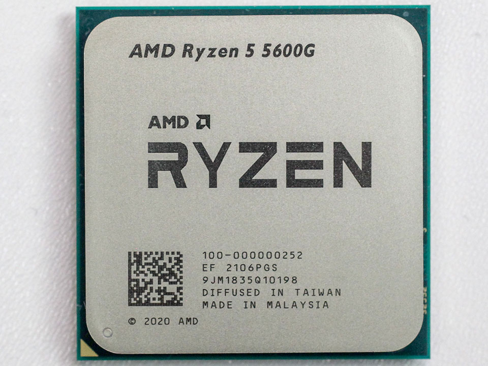

The processor looks like any conventional AMD CPU with a large IHS dominating the top and a 1,331-pin micro-PGA as the bottom. The whole processor die is made in Taiwan at TSMC.
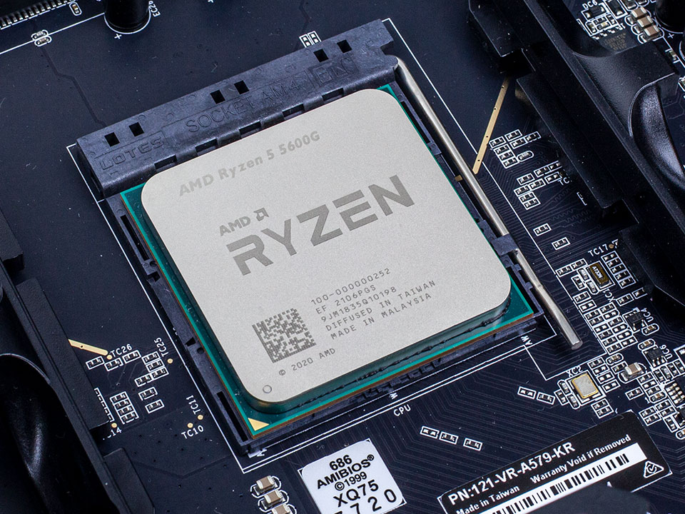
The Ryzen 5 5600G uses the same Socket AM4 as other Ryzens, so there's a huge selection of compatible coolers.
AMD Cezanne Silicon
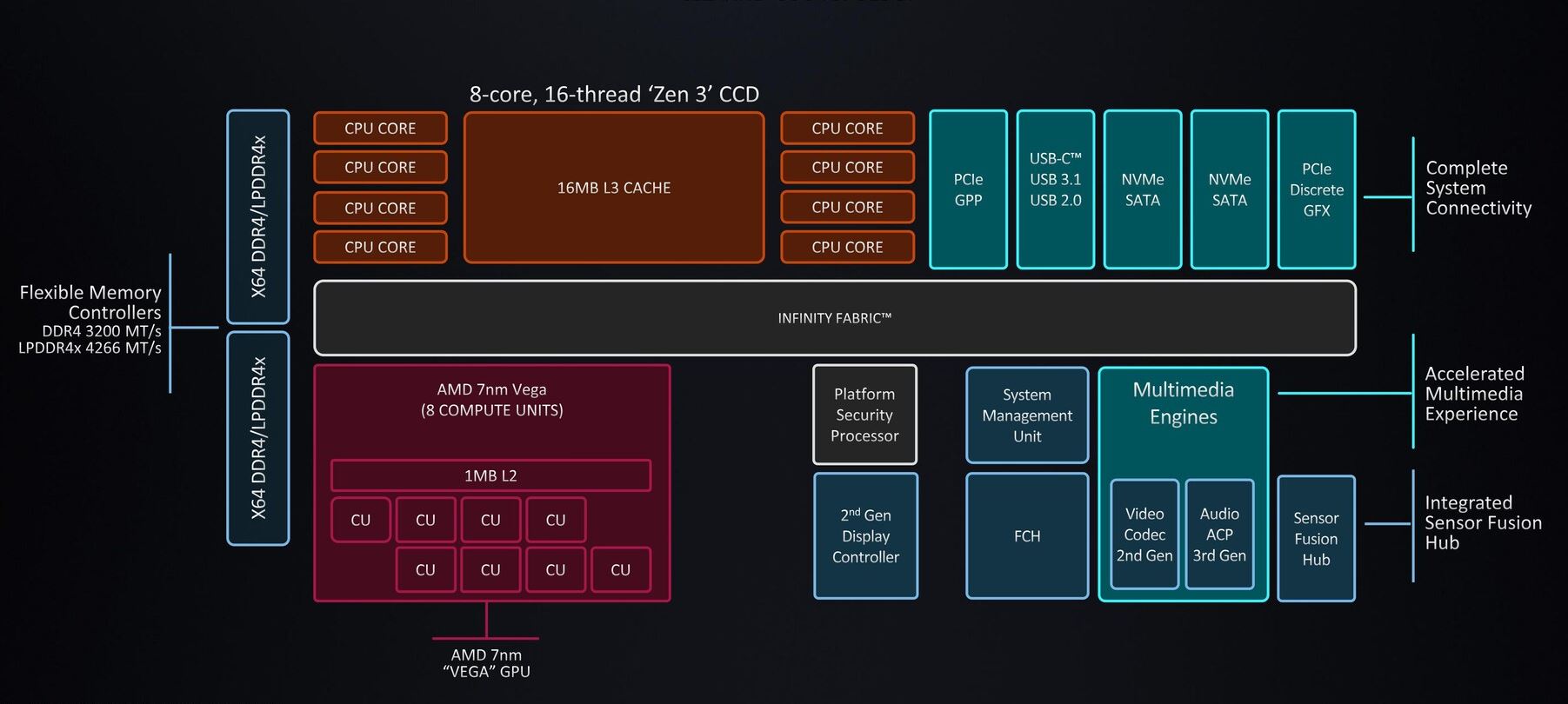
Unlike the other Ryzen 5000 desktop processors that are based on the Vermeer multi-chip module (MCM), the Ryzen 5000G processors with integrated graphics are based on a monolithic die codenamed "Cezanne." Built entirely on the 7 nm silicon fabrication process, it has a die area of 180 mm² with a transistor-count of 10.7 billion. Designed to be an SoC in its own right, Cezanne combines an 8-core CPU based on the Zen 3 microarchitecture with an iGPU based on Vega, along with a dual-channel DDR4 integrated memory controller and I/O based on PCI-Express Gen 3. The Ryzen 5 5600G is carved out of this silicon by disabling 2 out of 8 CPU cores, and 1 out of 8 iGPU compute units, resulting in an SoC with a 6-core/12-thread CPU and 448 stream processors for the iGPU.
The biggest change Cezanne brings over last year's "Renoir" silicon (which did not launch in the retail segment) is the CPU. Besides the individual IPC gain, the eight cores now sit in a single, large CCX (CPU core complex) rather than being split up into two 4-core CCX. The biggest gain from this is that all eight cores now share a single 16 MB L3 cache. This effectively doubles the addressable L3 cache over the previous generation. The iGPU is largely carried over from Renoir with feature touch-ups to its display and media-acceleration components. The memory controller has been updated to support higher memory frequencies. It natively supports DDR4-3200 (compared to DDR4-2933 with Renoir) but, more importantly, handles higher memory overclocks. The only technological let-down is PCIe. AMD continues with Gen 3 PCIe, which is a big missed opportunity to add Gen 4 given Intel extends Gen 4 I/O to even its mid-tier Core i5 "Rocket Lake" parts.
The Zen 3 Microarchitecture

Since its 2017 debut, AMD has delivered a new iteration of its groundbreaking "Zen" CPU microarchitecture each year, each with IPC improvements. As we mentioned earlier, the new Zen 3 microarchitecture claims to offer a massive 19 percent IPC uplift over its predecessor, Zen 2. This is accomplished by improvements at both the micro and macro levels. We already detailed the macro (beyond the core) changes above. In this section, we talk about what's new inside each core. AMD mentioned updates to practically all key components of the core, including its front-end, fetch/decode, integer and floating-point components, load-store, and dedicated caches. Just to clarify, this component is unchanged compared to other Zen 3 CPUs without an IGP, like the Ryzen 9 5900X.
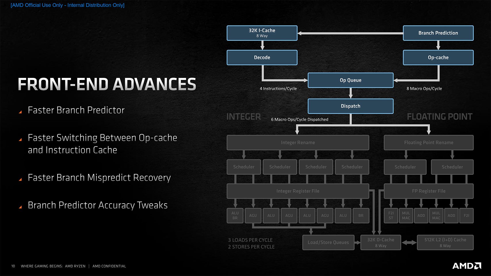
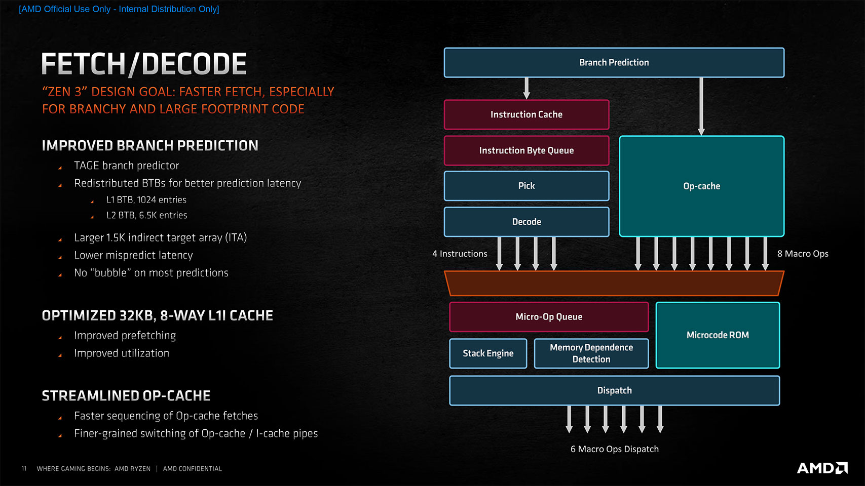
Modern processors execute multiple instructions in parallel to improve performance. Computer programs consist of huge amounts of "if ... then ... else" instructions, which slow down the processor because it has to evaluate the condition before picking a branch to execute. In order to overcome this limitation, the branch predictor was invented, a piece of circuitry that takes a guess on the more likely outcome of the condition check and just speculatively executes that branch's instructions. Of course, there's a chance that the prediction is wrong, in which case a performance penalty is incurred from undoing the executions that were already executed. With Zen 3, AMD uses an improved TAGE branch predictor, which is more accurate and recovers faster from mispredictions. They also changed the design to be "bubble free," which avoids inserting "wait for result" instructions into the instruction stream whenever a branch is encountered.
AMD generally increased operations per cycle; the front end now switches between the op and instruction caches faster. The 32 KB L1 instruction cache has been tweaked to offer better utilization due to efficient tagging and pre-fetching. Streamlining was done to the Op cache. Improvements to the branch predictor and front end add up to nearly a quarter of the overall 19% generational IPC uplift.

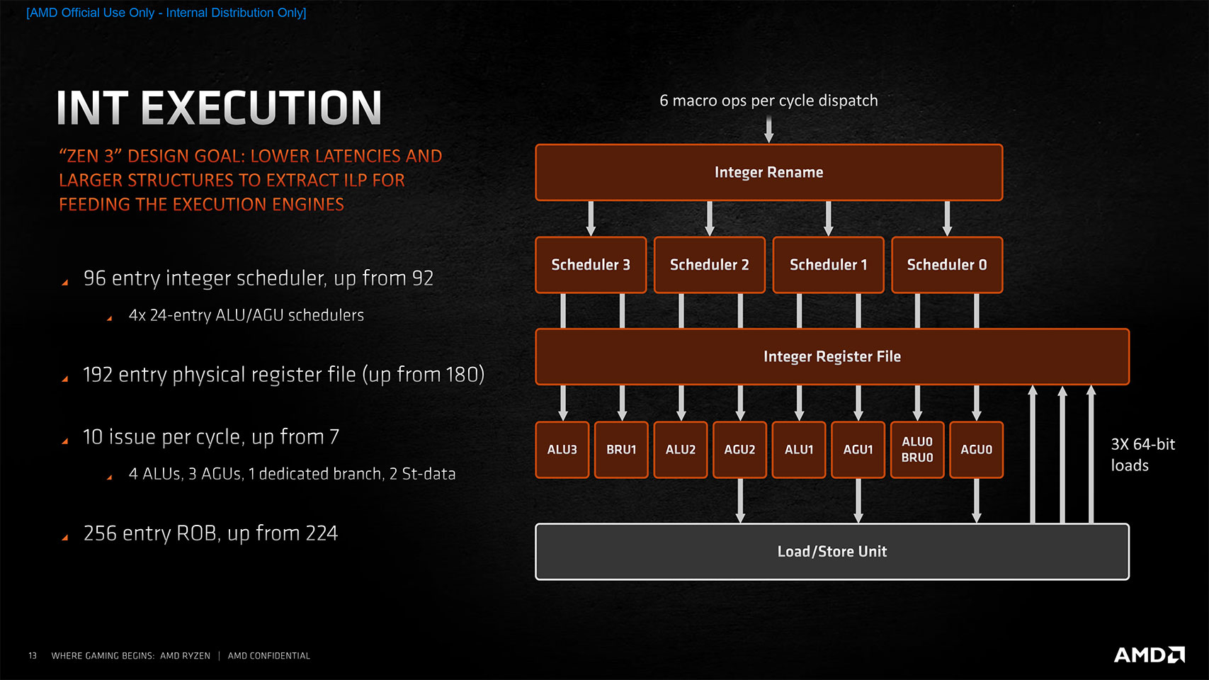
The execution engine, or combination of the integer and floating-point execution units, is the main math muscle of the CPU core. The Zen 3 microarchitecture features improvements to both over Zen 2. Both the INT and FP issue queues, which feed work to the two engines, have been widened and the execution window enlarged. This ensures fewer units are idle in typical programs, which increases overall performance.

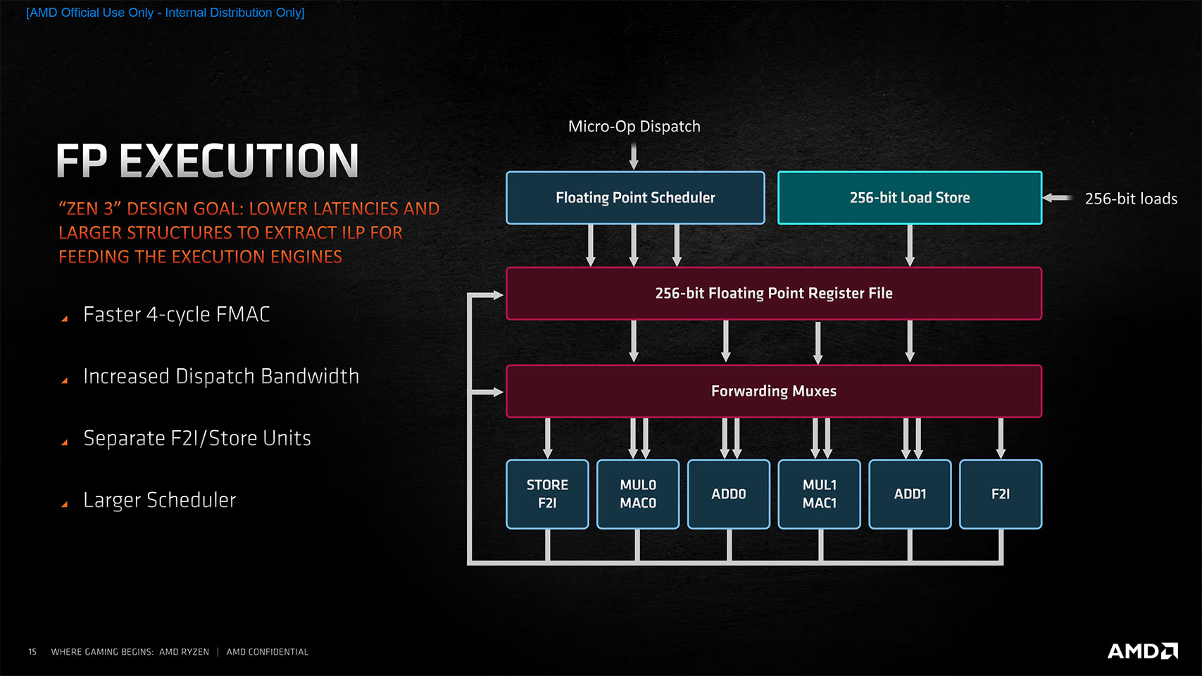
AMD worked to minimize latencies at every stage of the INT execution engine and enlarged its key structures, including the integer scheduler (96 entry vs. 92 on Zen 2), physical register file (192 vs. 180 on Zen 2), and 10 issues per cycle, up from 7 on Zen 2. Data picker bandwidth has been significantly increased despite the same number of ALUs. The floating-point engine features the same 256-bit FPUs, but just as with the INT engine, the FP engine has latency and bandwidth improvements across the board, faster 4-cycle FMAC, and larger scheduler. The INT and FP improvements contribute around a fifth of the 19% overall IPC uplift.

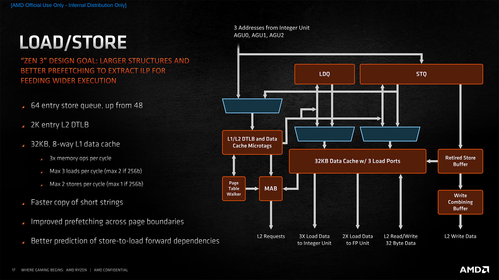
With the Zen 3 microarchitecture, AMD addressed many bottlenecks and "intelligence" issues with the Load/Store unit. The biggest has to be bandwidth. The entry store queue has been widened to 64 from 48 on Zen 2, and the L2 cache DTLB is 2K entries wide. The 32 KB L1 data cache has been made faster with lower latencies. Memory dependence detection has been improved. Much like the front end and scheduler, the load/store improvements contribute nearly a quarter of the 19% overall IPC uplift, meaning that by just optimizing the non-execution components of its core, AMD managed to pull off a vast 9% overall IPC uplift.
ISA and Security Changes

Each new microarchitecture heralds support for newer instruction sets and security hardening, and the same is the case with Zen 3; however, a notable absentee is AVX-512. Granted, Intel has adopted a less than perfect method of proliferating AVX-512 with certain instructions being exclusive to enterprise-segment microarchitectures and only a handful client-relevant instructions on its "Ice Lake" and "Tiger Lake" architectures, but there's no movement from AMD in this direction.
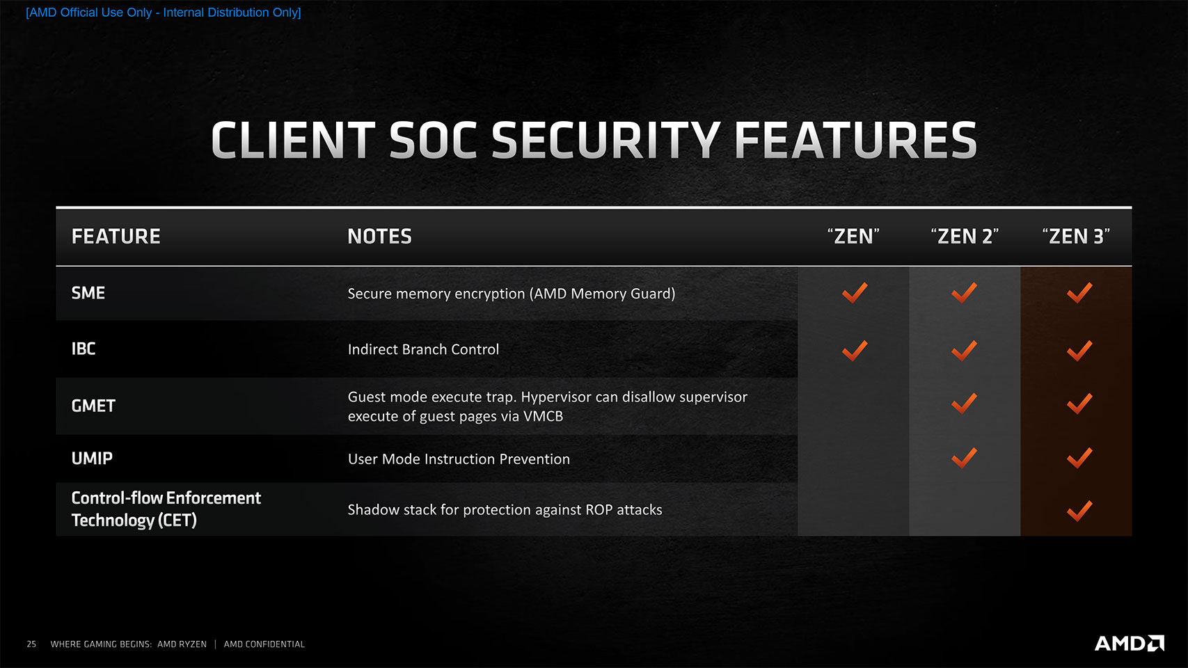
You still do get 256-bit instructions from within the AVX2 set. Also missing in action is something to rival Intel's DLBoost, which is essentially a software exposure of fixed-function hardware that accelerates matrix multiplication, in effect AI deep-learning neural net building and training. A lot of client applications, particularly image manipulation and video editing, are leveraging edge AI, and some investment from AMD on this would have been nice. That said, Zen 3 adds two new ISA instructions, MPK (memory protection keys) and AVX2 support for AES/APCLMulQD. AMD has been ahead of Intel with CPU core security vulnerability perception, and with Zen 3, AMD is introducing CET, or control-flow enforcement, which should provide hardening against ROP-type attacks.
Integrated Radeon Vega Graphics
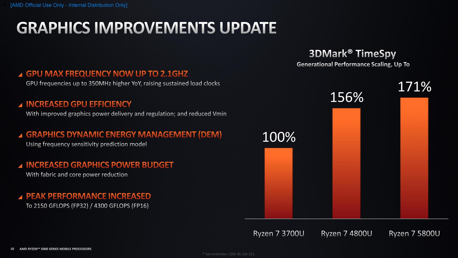
The raison d'etre of the Ryzen 5000G series is its integrated graphics, something not found on other Ryzen 5000 series desktop processors. The AMD Cezanne silicon integrates an iGPU based on the same old Vega architecture, but with some improvements. Why AMD went with Vega and not at least RDNA1 is anyone's guess. The company is probably looking to conserve silicon real estate and thinks it can improve its performance to stay ahead of Rocket Lake, and its Gen12 Xe iGPU. The iGPU is mostly unchanged from the previous-generation Renoir. It still only has up to 8 compute units (512 stream processors), 64 TMUs, and 8 ROPs and relies entirely on the system memory share. AMD updated a few things, however. These include a reworked power delivery system to the iGPU and reduced Vmin (minimum core voltage), 350 MHz increase in engine clocks that are sustained better, and other improvements related to fabric and CU power. These power efficiency improvements convert to an increased power budget, letting the iGPU sustain higher engine clocks better.
AMD X570 and B550 Chipsets

At launch, Ryzen 5000 Zen 3 processors should be compatible with all Socket AM4 motherboards based on AMD X570 and B550 chipsets, with a BIOS update that has the latest AGESA ComboPI 1.1.0.0 micro-code. The BIOS update must be installed before installing the Zen 3 CPU. Trying to boot the old BIOS with a Zen 3 will not work (we've tried). Luckily, most Socket AM4 motherboards feature some form of USB BIOS flashback feature that lets you update the motherboard BIOS without having to install a processor or memory, which means you won't have to borrow an older processor just to update your motherboard's BIOS. Recent batches of AMD 500-series chipset motherboards should ship with Ryzen 5000 series support out of the box.
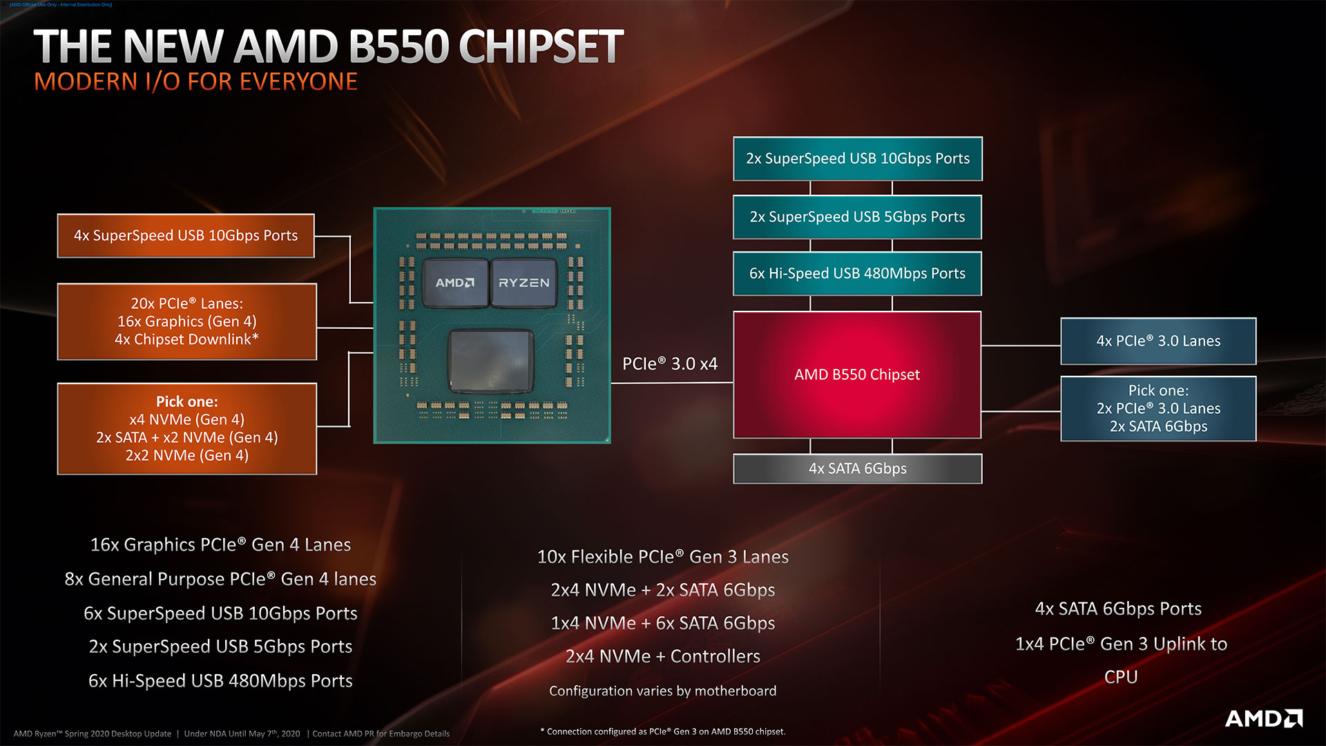
The AMD X570 chipset is a premium offering that enables PCI-Express gen 4.0 not just from the processor (i.e., the main x16 PEG slot and one M.2 NVMe slot), but also downstream PCIe lanes attached to the chipset. You get up to 16 PCIe Gen 4 lanes from the chipset, which can be re-configured as SATA or USB3 ports by the motherboard designer. The B550 chipset lets you have one PCIe Gen 4 main x16 slot and one M.2 NVMe slot, but all chipset-attached downstream lanes are PCIe gen 3. The B550 puts out eight downstream lanes. When paired with 5000G Cezanne processors, the downstream PCIe lanes of the X570 operate at Gen 3 speeds despite being capable of Gen 4.
Our Patreon Silver Supporters can read articles in single-page format.
Apr 26th, 2024 02:21 EDT
change timezone
Latest GPU Drivers
New Forum Posts
- What's your latest tech purchase? (20342)
- What phone you use as your daily driver? And, a discussion of them. (1483)
- Best SSD for system drive (81)
- AMD RX 7000 series GPU Owners' Club (1087)
- im new to throttelstop and i think i messed it up by copying others any hints would be very much aprreciated (3)
- Horizontal black lines popping up on my screen? (4)
- Which new games will you be buying? (316)
- Alphacool CORE 1 CPU block - bulging with danger of splitting? (20)
- Black screen after muting (5)
- What are you playing? (20530)
Popular Reviews
- Fractal Design Terra Review
- Thermalright Phantom Spirit 120 EVO Review
- Corsair 2000D Airflow Review
- ASUS GeForce RTX 4090 STRIX OC Review
- NVIDIA GeForce RTX 4090 Founders Edition Review - Impressive Performance
- ASUS GeForce RTX 4090 Matrix Platinum Review - The RTX 4090 Ti
- MSI GeForce RTX 4090 Suprim X Review
- Gigabyte GeForce RTX 4090 Gaming OC Review
- MSI GeForce RTX 4090 Gaming X Trio Review
- MSI GeForce RTX 4090 Suprim Liquid X Review
Controversial News Posts
- Sony PlayStation 5 Pro Specifications Confirmed, Console Arrives Before Holidays (117)
- Windows 11 Now Officially Adware as Microsoft Embeds Ads in the Start Menu (112)
- NVIDIA Points Intel Raptor Lake CPU Users to Get Help from Intel Amid System Instability Issues (106)
- AMD "Strix Halo" Zen 5 Mobile Processor Pictured: Chiplet-based, Uses 256-bit LPDDR5X (101)
- US Government Wants Nuclear Plants to Offload AI Data Center Expansion (98)
- AMD's RDNA 4 GPUs Could Stick with 18 Gbps GDDR6 Memory (88)
- Developers of Outpost Infinity Siege Recommend Underclocking i9-13900K and i9-14900K for Stability on Machines with RTX 4090 (85)
- Windows 10 Security Updates to Cost $61 After 2025, $427 by 2028 (84)