 53
53
AMD Ryzen 7 3800XT Review
Test Setup »Architecture
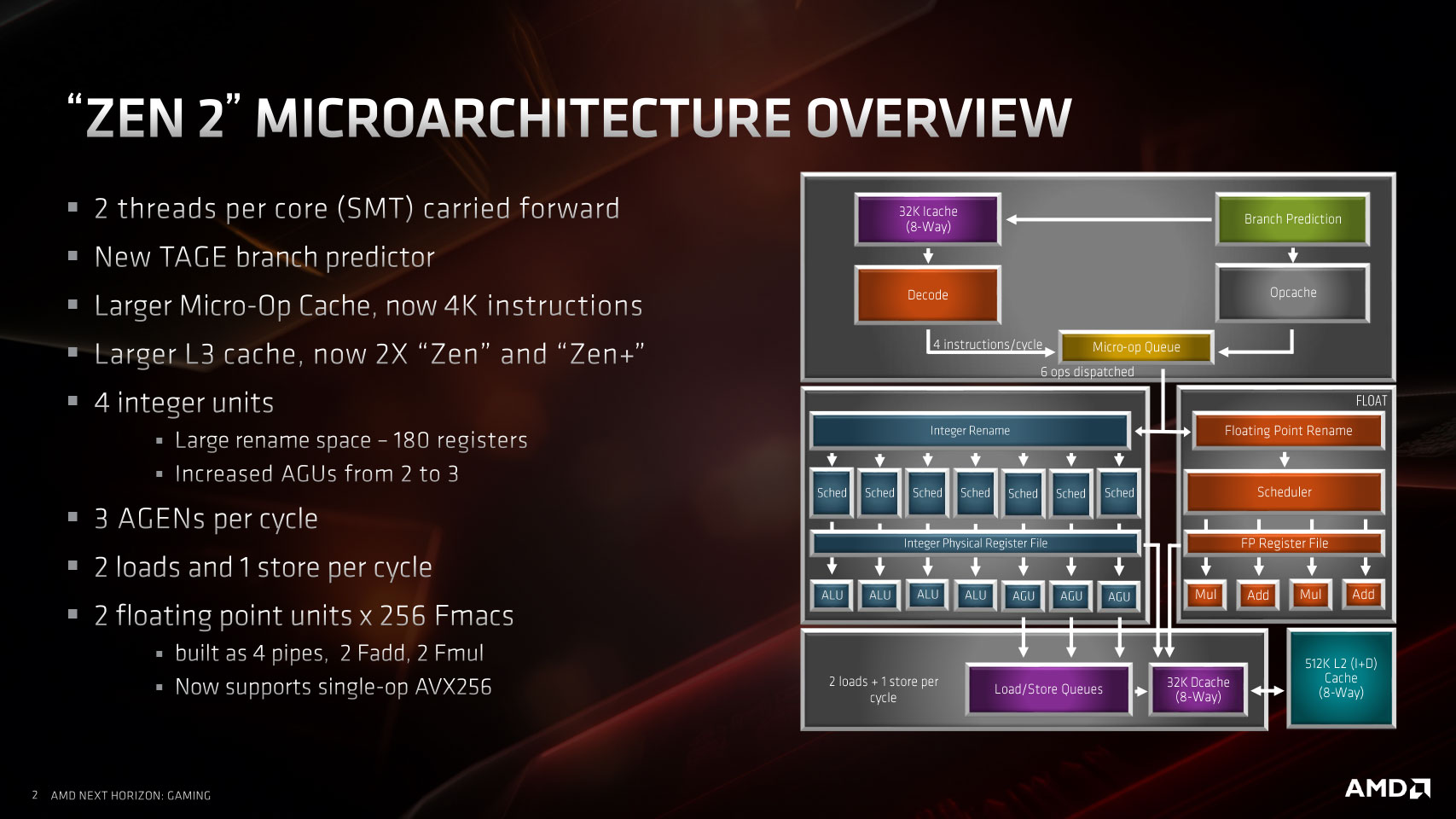
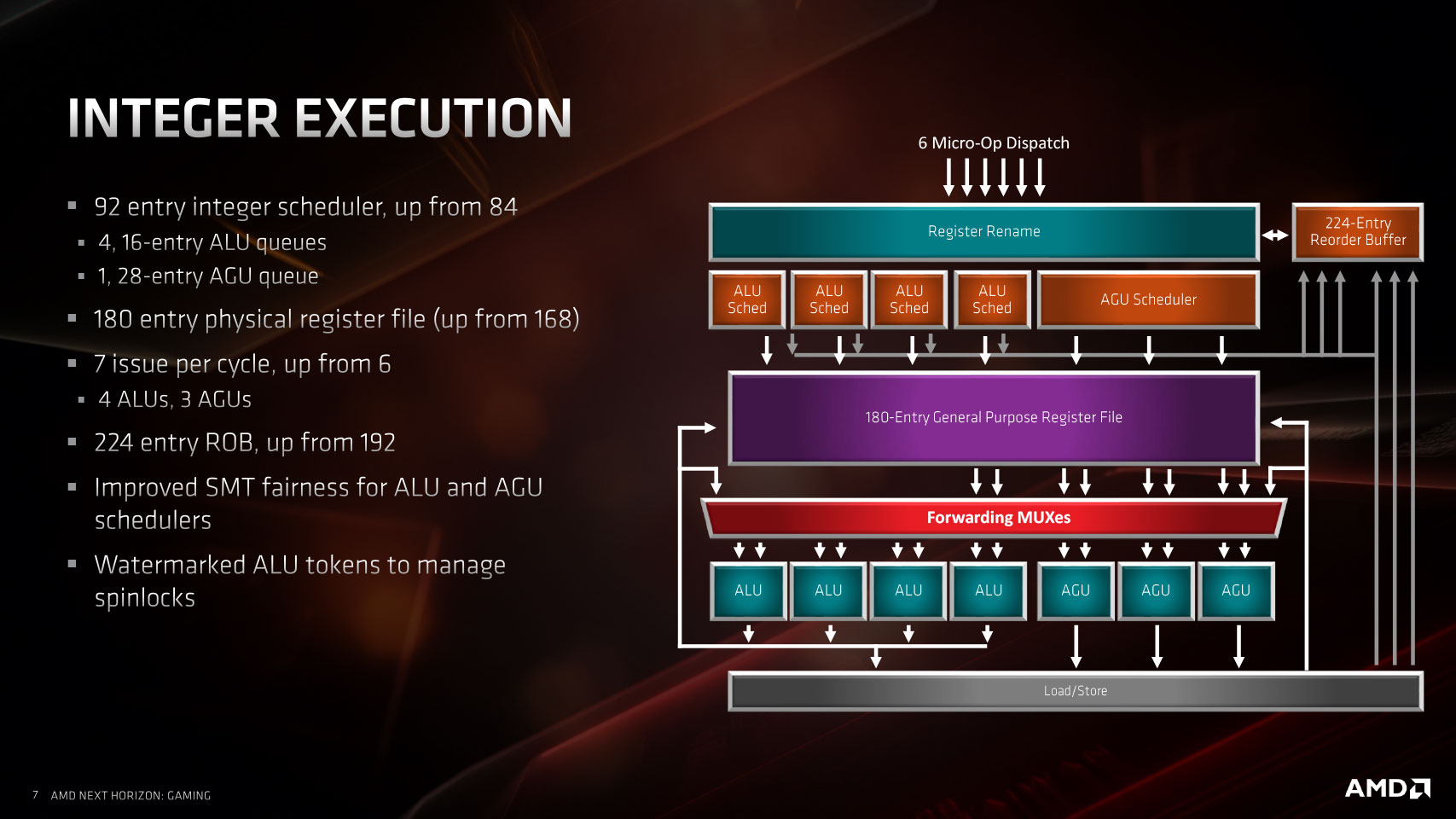
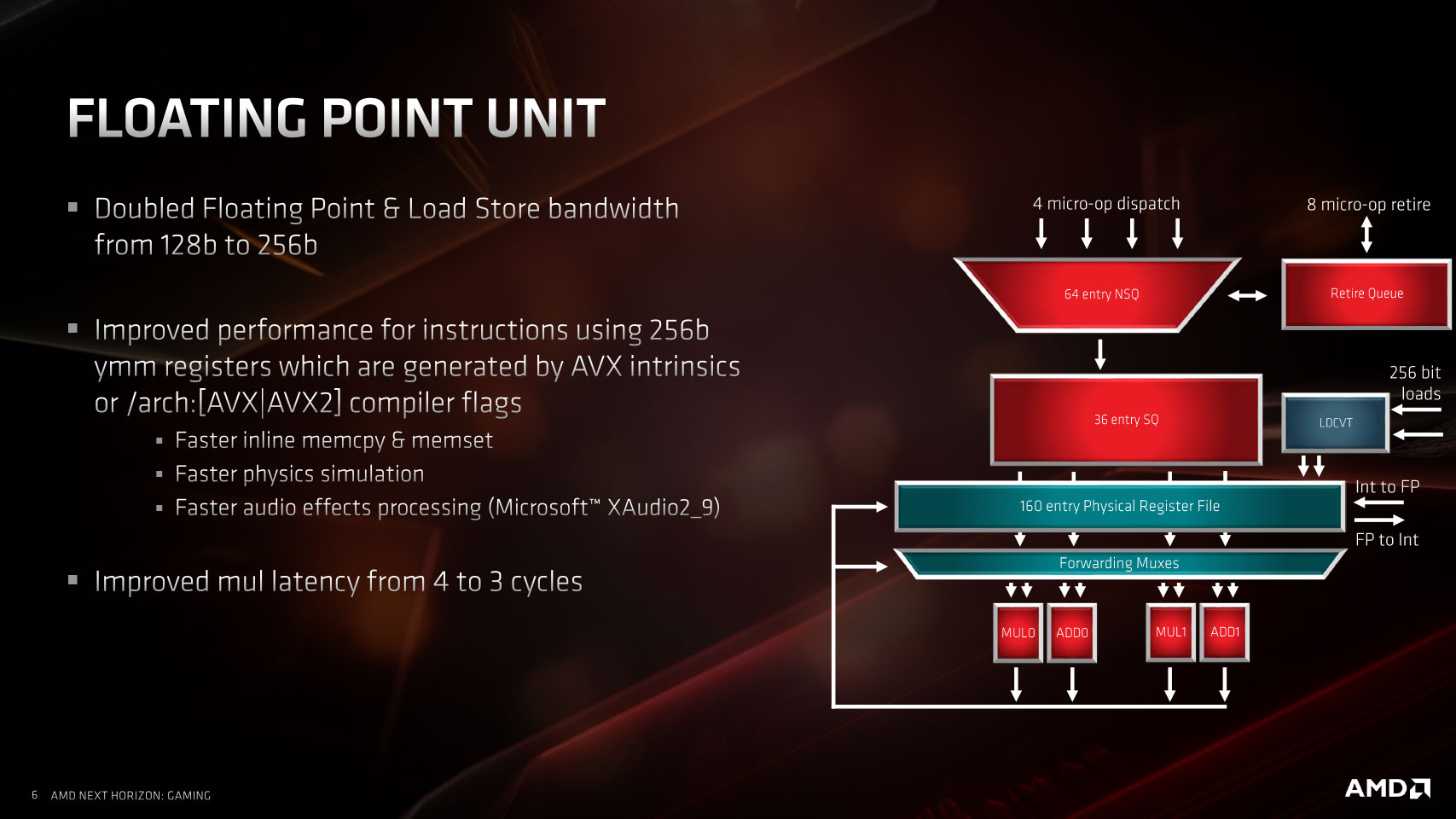
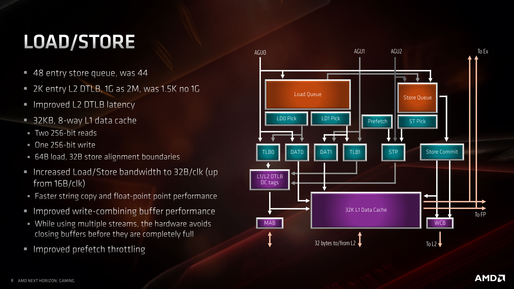
The architecture is no different from the Ryzen 9 3950X or any other "Matisse," so you can click on the button below to read about it, or skip that section if you're familiar with it.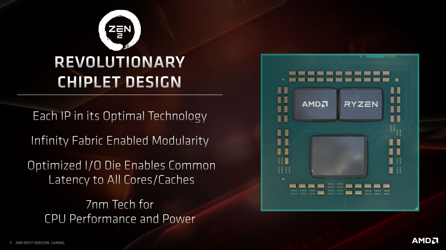


Architectural Innovations Specific to Ryzen 3000XT Series
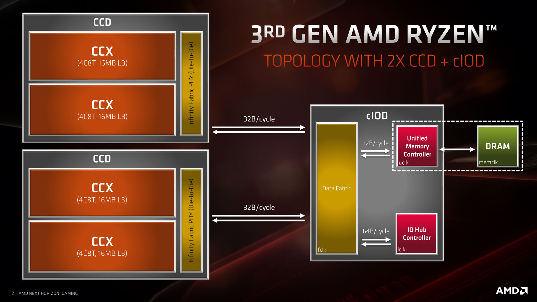
AMD internally refers to the Ryzen 3000XT family of processors as "Matisse 2." These are almost identical to the original Ryzen 3000 "Matisse" processors based on the "Zen 2" microarchitecture, but AMD has given these processors some physical improvements. To begin with, the 8-core CCDs (compute complex dies) or "Zen 2" chiplets inside the processors are still based on TSMC N7 (the foundry's first 7 nm node), but with certain refinements. AMD claims these yields a single-digit percentage electrical improvement, which AMD uses to achieve up to 200 MHz increments in maximum boost frequencies without it affecting the TDP of these processors.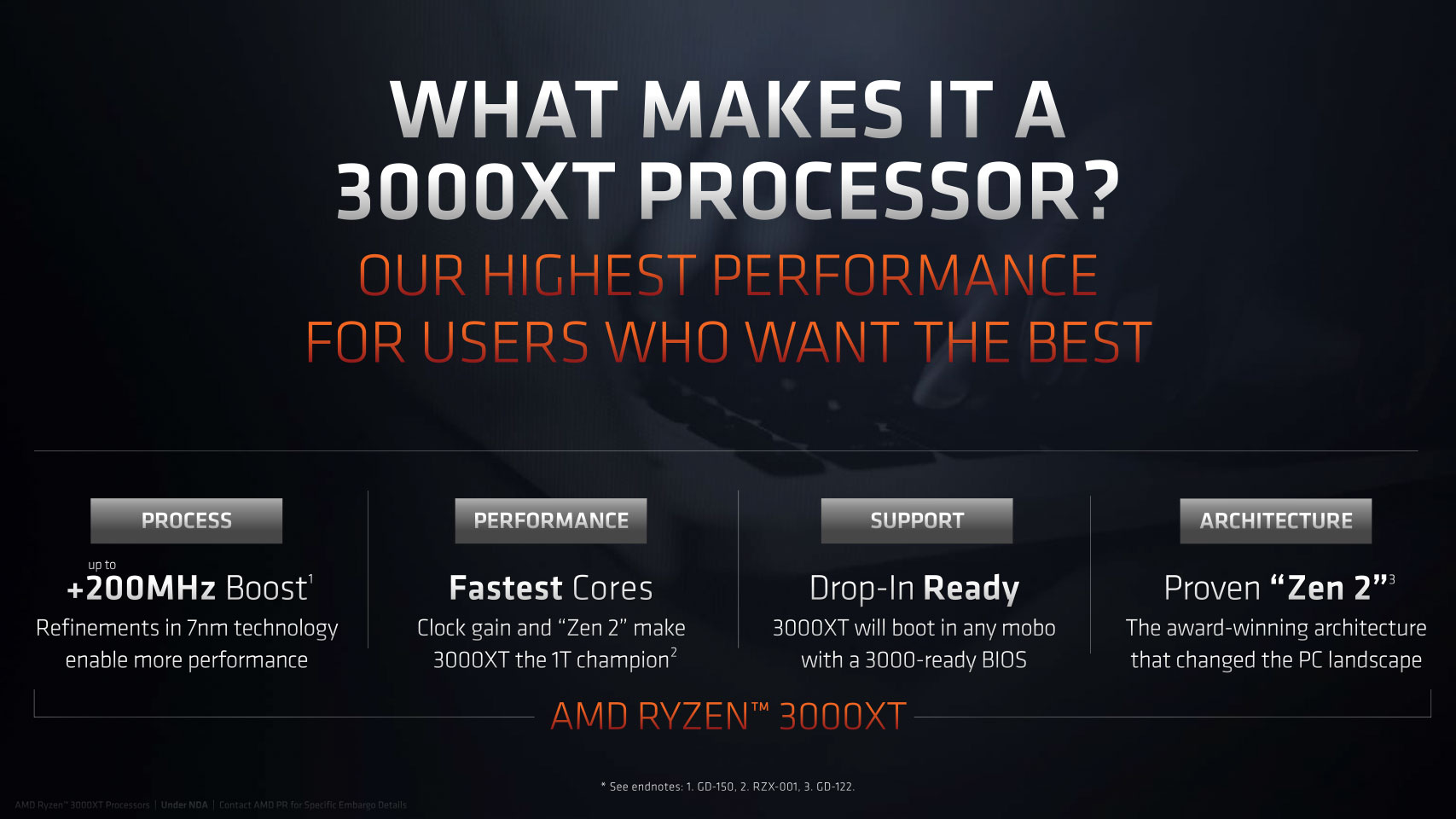
The TDP of Ryzen 5 3600XT remains at 95 W, just like the 3600X, while both the 3800XT and 3900XT stick with 105 W TDP. AMD's decision not to include cooling solutions with the 3800XT and 3900XT have little to do with the power or thermals of these processors and more with marketing decisions taken by AMD. It certainly reduces AMD's bill of materials for these chips.
AMD categorically stated that this "refined" N7 node is neither N7P nor N7+. The N7P node is the successor to N7 that sticks to DUV (deep ultraviolet) lithography, but innovates in certain other areas to eke out a power improvement. N7+, on the other hand, uses EUV (extreme ultraviolet) lithography that not only yields much higher efficiency, but also over a 20% increase in transistor-density. The node AMD is building "Matisse 2" on is still N7, but with certain refinements AMD didn't elaborate in its product brief.
AMD B550 and X570 Chipsets
With premium AMD X570 chipset-based motherboards starting at $150, it's less likely that someone would pair the third-generation Ryzen 3 with it. Choosing a cheaper B450 motherboard would mean giving up on killer features such as PCIe gen 4.0. AMD hence launched the new B550 mid-range chipset alongside these processors. The B550 chipset lets you have PCI-Express gen 4.0 connectivity from the "Matisse" processor, while limiting general-purpose PCIe downstream connectivity to gen 3.0.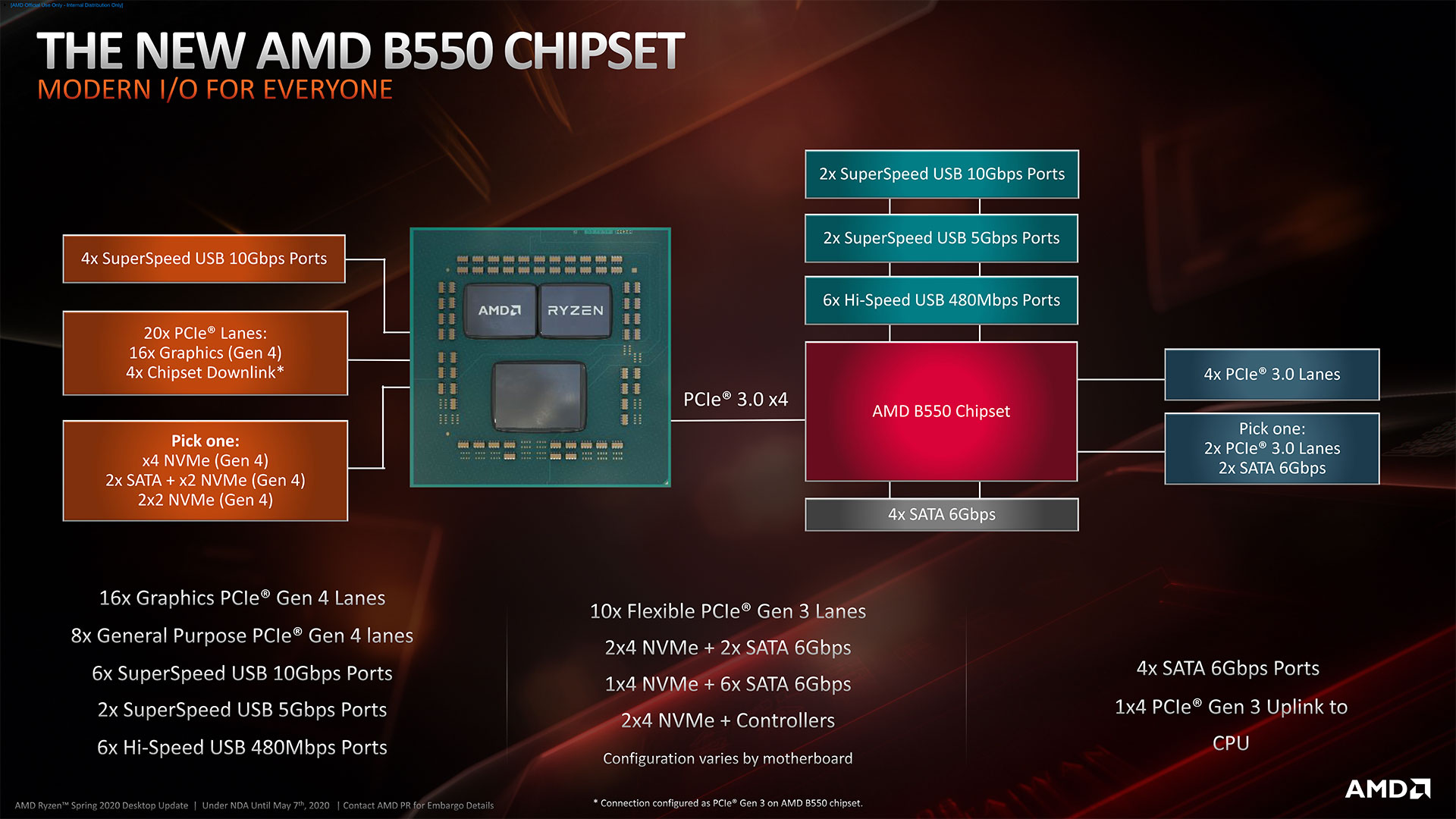
On a typical B550 chipset motherboard, the main PCI-Express x16 slot will be gen 4.0 if paired with a third-generation Ryzen "Matisse" processor, as would one of the board's M.2 NVMe slots that's wired to the processor. All other PCIe or M.2 slots which are wired to the B550 chipset will be gen 3.0. This way, future-proofing of the platform for next-generation graphics cards and SSDs remains intact. The B550 chipset provides up to six SATA 6 Gbps ports with AHCI and RAID capability, up to two 10 Gbps USB 3.1 gen 2 ports (in addition to four such ports put out by the "Matisse" processor), two additional USB 3.1 gen 1 ports, and six USB 2.0 ports. The platform's HDA and LPCIO buses are located on the processor.

A word on compatibility. The B550 chipset only supports third-generation Ryzen "Matisse" processors as of this writing, and AMD confirmed support for next-generation processors based on the "Zen 3" architecture. You cannot pair a B550 motherboard with older Ryzen 2000/1000 processors or even the 3200G or 3400G APUs based on the older "Zen+" microarchitecture. There will be clear labeling on B550 chipset motherboard boxes to this effect.
What we like most about the B550 is its low TDP, which lets motherboard designers make do with passive heatsinks; unlike X570, which requires active fan heatsinks.

AMD delivered on its promise of third-generation Ryzen "Matisse" processors being backwards compatible with older Socket AM4 motherboards, going all the way back to the AMD 300-series chipset, with a simple BIOS update. To make the most out of Ryzen "Matisse"—namely, PCI-Express gen 4.0 connectivity and increased CPU/memory overclocking headroom, you're expected to use one of the latest motherboards that use the AMD X570 chipset. The X570 is an entirely different chip from X470 and X370. The older chipsets were supplied by ASMedia and were rather slim in their downstream connectivity.
The X470 only puts out 8 PCIe gen 2.0 downstream lanes, for example. The X570 modernizes all I/O by putting out up to 16 PCIe gen 4.0 downstream lanes. This enables additional M.2 PCIe gen 4 slots on your motherboards for the latest SSDs featuring PCIe gen 4 support and creates room for many new bandwidth-hungry onboard devices, such as 10 GbE adapters, next-generation Thunderbolt, 802.11ax controllers, etc. Along with the "Matisse" SoC, the X570 also puts out a number of 10 Gbps USB 3.1 gen 2 ports. Motherboards based on X570 also implement modern network connectivity options, such as 2.5 GbE and 802.11ax WLAN.
Given there are highly capable motherboards based on the B550 chipset with serious VRM solutions and high-end connectivity, it's good enough for any Ryzen 3000XT series processor, including the 3900XT. The B550 chipset also offers multi-GPU support. Your choice between the B550 and X570 should hence boil down to whether you plan to have more than one M.2 NVMe SSD that can take advantage of PCI-Express gen 4.0, or an NVMe RAID setup of 2–3 PCIe gen 4.0-capable M.2 SSDs. Serious overclockers should still consider the X570 since the most beastly VRM setups are still found on boards such as the MSI MEG X570 GODLIKE, ASUS ROG Crosshair VII Formula, and GIGABYTE X570 AORUS Xtreme.
AMD StoreMI 2.0 Technology

AMD today is also debuting the second generation StoreMI technology, a value addition to its Socket AM4, TR4, and sTRX4 platforms. StoreMI is a free software for AMD users which allows you to build volumes that span across multiple storage devices, such as SSDs and HDDs. Depending on the "heat" (frequency of access) of the data, the software decides what data to store in the fastest media. Unlike the original StoreMI technology that debuted with AMD's 400-series chipset, StoreMI 2.0 is an in-house development by AMD and improves on an important front—the software doesn't physically move data between various storage devices. Rather, depending on available space and heat, it copies data from the slower media to the faster one, and points the OS to the copy that's on the faster media. This way, there's no scope for data loss. AMD also redesigned the user interface.
Apr 25th, 2024 07:12 EDT
change timezone
Latest GPU Drivers
New Forum Posts
- (Anti) SFF fun house (353)
- Last game you purchased? (255)
- Core i5-6300U (16)
- Share your AIDA 64 cache and memory benchmark here (2916)
- What phone you use as your daily driver? And, a discussion of them. (1472)
- What's your latest tech purchase? (20338)
- Meta Horizon OS (16)
- Alphacool CORE 1 CPU block - bulging with danger of splitting? (4)
- The TPU UK Clubhouse (24786)
- Github comments used to push malware via Microsoft repo urls (3)
Popular Reviews
- Fractal Design Terra Review
- Thermalright Phantom Spirit 120 EVO Review
- Corsair 2000D Airflow Review
- Minisforum EliteMini UM780 XTX (AMD Ryzen 7 7840HS) Review
- ASUS GeForce RTX 4090 STRIX OC Review
- NVIDIA GeForce RTX 4090 Founders Edition Review - Impressive Performance
- ASUS GeForce RTX 4090 Matrix Platinum Review - The RTX 4090 Ti
- MSI GeForce RTX 4090 Suprim X Review
- MSI GeForce RTX 4090 Gaming X Trio Review
- Gigabyte GeForce RTX 4090 Gaming OC Review
Controversial News Posts
- Sony PlayStation 5 Pro Specifications Confirmed, Console Arrives Before Holidays (116)
- NVIDIA Points Intel Raptor Lake CPU Users to Get Help from Intel Amid System Instability Issues (106)
- AMD "Strix Halo" Zen 5 Mobile Processor Pictured: Chiplet-based, Uses 256-bit LPDDR5X (101)
- US Government Wants Nuclear Plants to Offload AI Data Center Expansion (98)
- Windows 11 Now Officially Adware as Microsoft Embeds Ads in the Start Menu (84)
- Windows 10 Security Updates to Cost $61 After 2025, $427 by 2028 (84)
- Developers of Outpost Infinity Siege Recommend Underclocking i9-13900K and i9-14900K for Stability on Machines with RTX 4090 (84)
- AMD's RDNA 4 GPUs Could Stick with 18 Gbps GDDR6 Memory (80)