 163
163
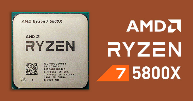
AMD Ryzen 7 5800X Review
(163 Comments) »Introduction
AMD today announced the Ryzen 5000-series "Zen 3" desktop processors, and we have with us the Ryzen 7 5800X 8-core processor in this review. The company skipped over the "4000"-series model numbering, probably because the numbers were cluttered by the "Renoir" APU silicon. With today's announcement, AMD keeps its promise of releasing a new generation of "Zen" CPU microarchitecture each year since its 2017 debut, and with each new generation, they introduced IPC increments. IPC, or instructions per clock, is a de-facto way of measuring the single-threaded performance of a processor and has a direct impact on gaming performance.
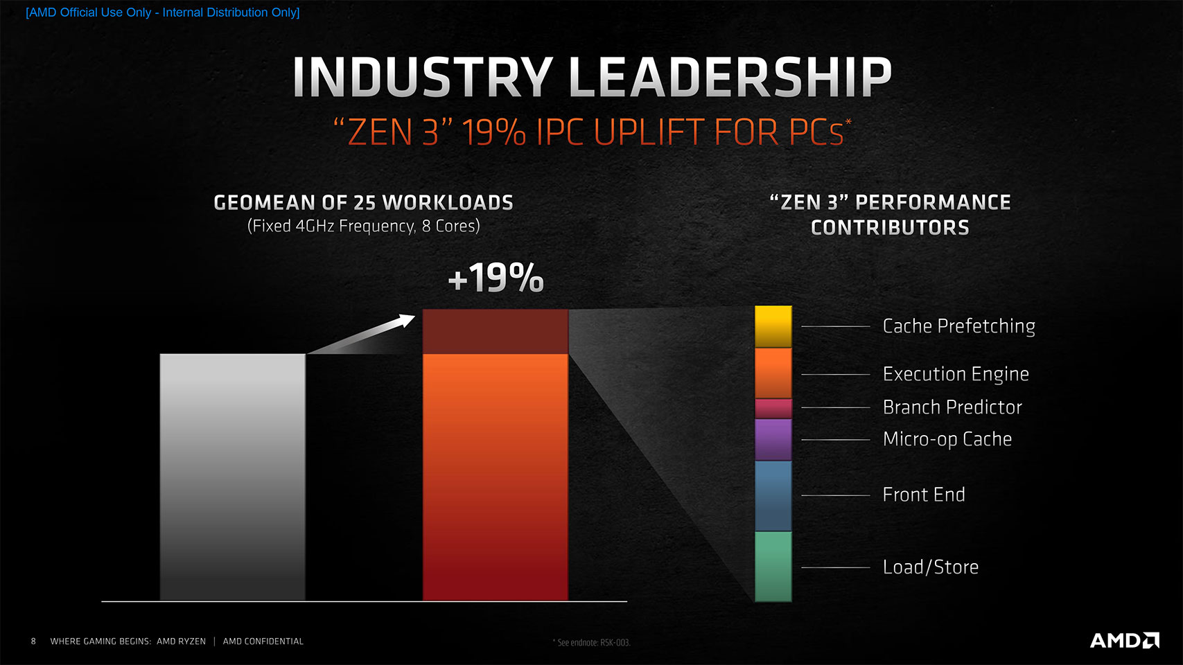
With "Zen 3," AMD is claiming an astounding 19% IPC increase over "Zen 2," in contrast to Intel's zero IPC gains in the desktop segment over the past half decade or so. Riding on the backs of these 19% IPC improvements is AMD's claim to have beaten Intel at gaming performance, given the Ryzen 3000 "Zen 2" wasn't too far behind Intel's 10th Gen Core "Comet Lake" at gaming. With productivity tasks, AMD's higher core counts for the Ryzen 9 series will give it the edge by virtue of higher core counts, 12-core and 16-core, but the game is evenly balanced when it comes to the Ryzen 7 5800X compared to its Intel rival, the Core i7-10700K, since both are 8-core/16-thread.
Much like the Core i7-10700K, the Ryzen 7 5800X in this review is a "monolithic" 8-core processor in that all its eight cores don't just sit on the same silicon, the "Zen 3" CCD, but also share a common L3 cache. AMD's Ryzen 5000 processors still implement a multi-chip module, with this generation's MCM being codenamed "Vermeer." The doing away of 4-core CCX complexes to unify cores on the CCD should pay dividends in the form of reduced inter-core latencies and effectively double L3 cache size each core can address.
AMD is announcing the Ryzen 7 5800 "Zen 3" 8-core processor at $449, which is a major step up from the $399 that its predecessor, the 3800X, launched at. The 5800X is being offered as a premium gaming desktop chip for gameplay at any resolution. The chip retains a modern PCI-Express 4.0 bus for next-gen graphics cards. What's even more interesting is that despite the IPC and clock-speed gains, the Ryzen 7 5800X is being launched with the same 105 W TDP rating as its predecessor, and on the same 7 nm silicon fabrication node. In this review, we take the processor for a spin. We're especially looking forward to testing AMD's gaming performance claims.
| Price | Cores / Threads | Base Clock | Max. Boost | L3 Cache | TDP | Architecture | Process | Socket | |
|---|---|---|---|---|---|---|---|---|---|
| Ryzen 7 1800X | $250 | 8 / 16 | 3.6 GHz | 4.0 GHz | 16 MB | 95 W | Zen | 14 nm | AM4 |
| Core i7-8700K | $380 | 6 / 12 | 3.7 GHz | 4.7 GHz | 12 MB | 95 W | Coffee Lake | 14 nm | LGA 1151 |
| Core i7-9700K | $380 | 8 / 8 | 3.6 GHz | 4.9 GHz | 12 MB | 95 W | Coffee Lake | 14 nm | LGA 1151 |
| Core i7-10700K | $380 | 8 / 16 | 3.8 GHz | 5.1 GHz | 16 MB | 125 W | Comet Lake | 14 nm | LGA 1200 |
| Ryzen 7 3700X | $325 | 8 / 16 | 3.6 GHz | 4.4 GHz | 32 MB | 65 W | Zen 2 | 7 nm | AM4 |
| Ryzen 7 3800X | $340 | 8 / 16 | 3.9 GHz | 4.5 GHz | 32 MB | 105 W | Zen 2 | 7 nm | AM4 |
| Ryzen 7 3800XT | $380 | 8 / 16 | 3.9 GHz | 4.7 GHz | 32 MB | 105 W | Zen 2 | 7 nm | AM4 |
| Ryzen 7 5800X | $450 | 8 / 16 | 3.8 GHz | 4.7 GHz | 32 MB | 105 W | Zen 3 | 7 nm | AM4 |
| Core i9-10900 | $500 | 10 / 20 | 2.8 GHz | 5.2 GHz | 20 MB | 65 W | Comet Lake | 14 nm | LGA 1200 |
| Ryzen 9 3900X | $460 | 12 / 24 | 3.8 GHz | 4.6 GHz | 64 MB | 105 W | Zen 2 | 7 nm | AM4 |
| Ryzen 9 3900XT | $470 | 12 / 24 | 3.8 GHz | 4.7 GHz | 64 MB | 105 W | Zen 2 | 7 nm | AM4 |
| Ryzen 9 5900X | $550 | 12 / 24 | 3.7 GHz | 4.8 GHz | 64 MB | 105 W | Zen 3 | 7 nm | AM4 |
| Core i9-9900K | $390 | 8 / 16 | 3.6 GHz | 5.0 GHz | 16 MB | 95 W | Coffee Lake | 14 nm | LGA 1151 |
| Core i9-9900KS | $800 | 8 / 16 | 4.0 GHz | 5.0 GHz | 16 MB | 127 W | Coffee Lake | 14 nm | LGA 1151 |
| Core i9-10900K | $550 | 10 / 20 | 3.7 GHz | 5.3 GHz | 20 MB | 125 W | Comet Lake | 14 nm | LGA 1200 |
| Ryzen 9 3950X | $720 | 16 / 32 | 3.5 GHz | 4.7 GHz | 64 MB | 105 W | Zen 2 | 7 nm | AM4 |
| Ryzen 9 5950X | $800 | 16 / 32 | 3.4 GHz | 4.9 GHz | 64 MB | 105 W | Zen 3 | 7 nm | AM4 |
Unboxing and Photography
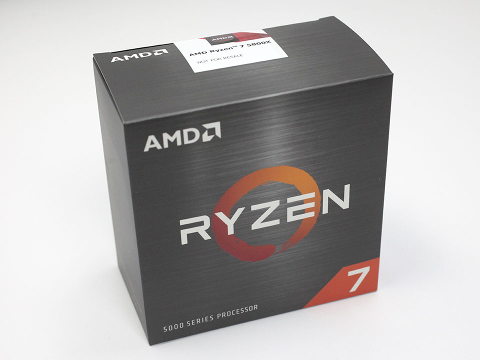
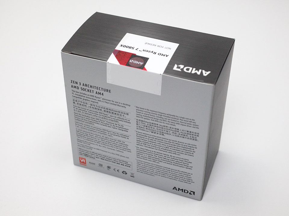
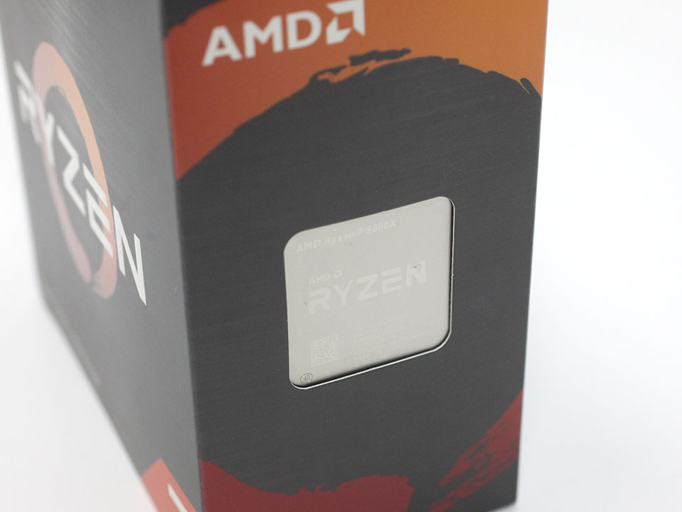
The Ryzen 7 5800X comes in a fairly large paperboard box. The front face of Ryzen 5000 series box features a brushed metal appearance (compared to the carbon fiber appearance of the Ryzen 3000 series). There are enough pointers to let you know you're buying a Ryzen 5000-series part. A small cutout on the side shows the actual processor inside the package.
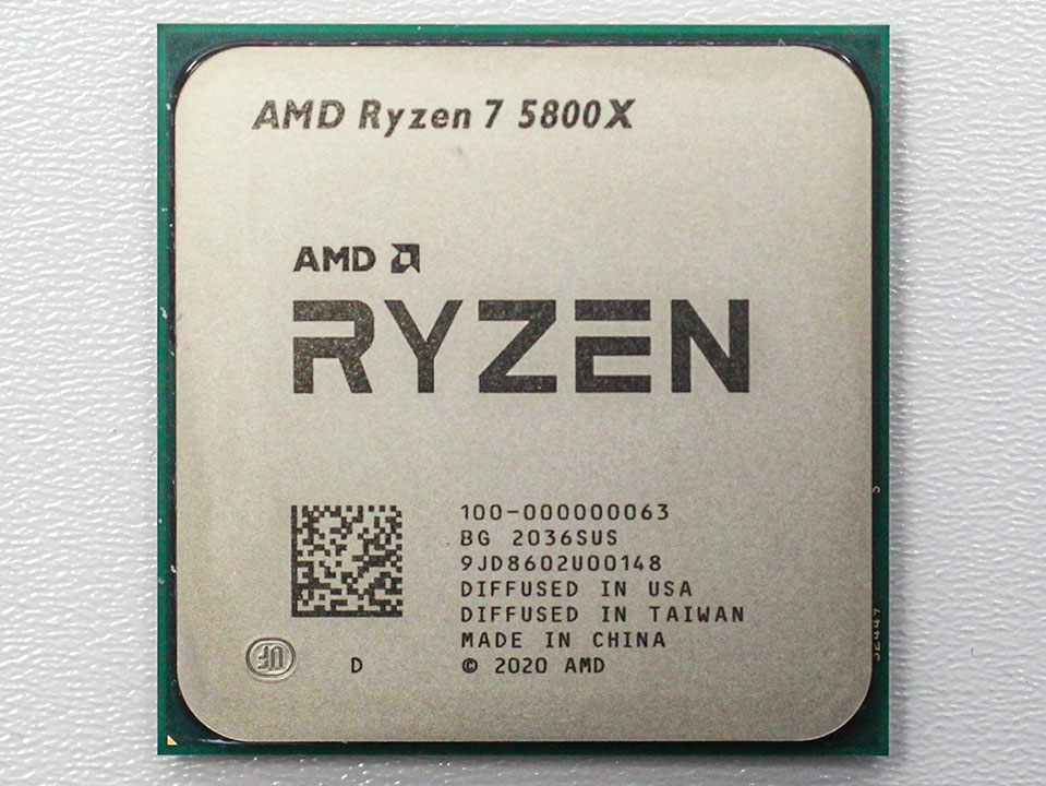
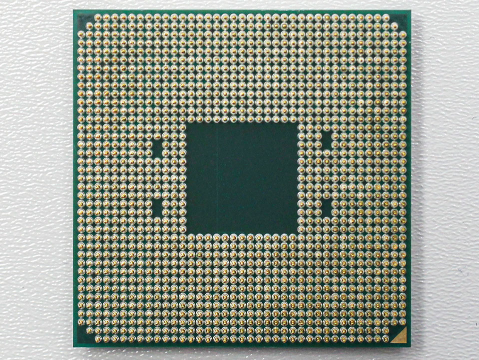
The processor looks like any conventional AMD CPU with a large IHS dominating the top, and a 1,331-pin micro-PGA as the bottom. The "Zen 3" CCD chiplet is made in Taiwan and the I/O die in the US, and the two are put together at a facility in China.

The retail Ryzen 7 5800X box does not include a cooler. Luckily, it can be paired with a fairly big selection of AM4-compatible coolers that have been released since 2017. Just make sure the cooler can handle thermal loads of 105 W.
Architecture
The Zen 3 Microarchitecture
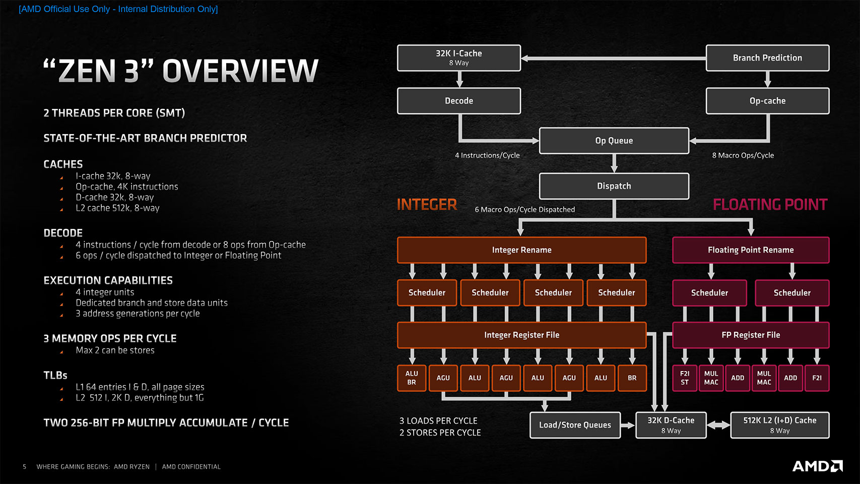
Since its 2017 debut, AMD has delivered a new iteration of its groundbreaking "Zen" CPU microarchitecture each year, each with IPC improvements. As we mentioned earlier, the new "Zen 3" microarchitecture claims to offer a massive 19 percent IPC uplift over its predecessor, "Zen 2." This is accomplished by improvements at both micro and macro levels. We already detailed the macro (beyond the core) changes above. In this section, we talk about what's new inside each core. AMD talks about updates to practically all key components of the core, including its front-end, fetch/decode, the integer- and floating-point components, load-store, and the dedicated caches.

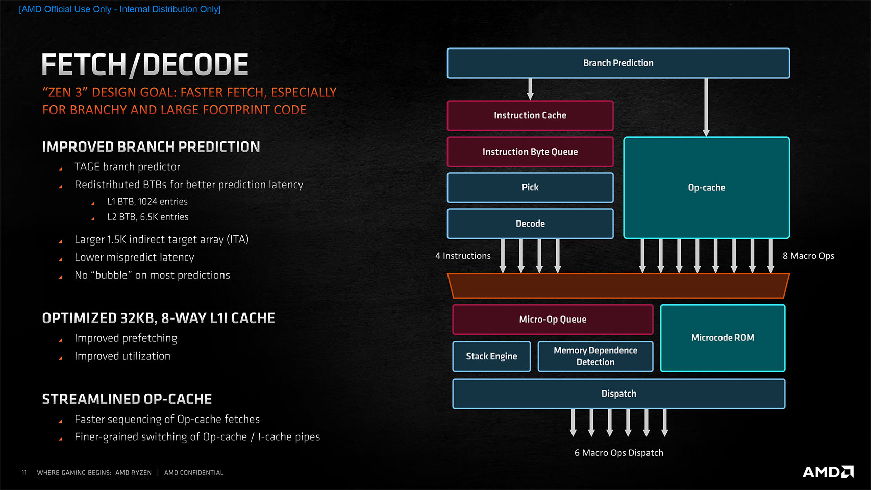
Modern processors execute multiple instructions in parallel to improve performance. Computer programs consist of huge amounts of "if ... then ... else" instructions, which slow down the processor because it has to evaluate the condition before picking a branch to execute. In order to overcome this limitation, the branch predictor was invented, a piece of circuitry that takes a guess on what's the more likely outcome of the condition check and just speculatively executes that branch's instructions. Of course, there's a chance that the prediction is wrong, in which case a performance penalty is incurred from undoing the executions that were already executed. With "Zen 3", AMD uses an improved TAGE branch predictor, which is more accurate and recovers faster from mispredictions. They also changed the design to be "bubble free," which avoids inserting "wait for result" instructions in the instruction stream whenever a branch is encountered.
AMD generally increased ops/cycle; the front-end now switches between the op and instruction caches faster. The 32 KB L1 instruction cache has been tweaked to offer better utilization due to efficient tagging and pre-fetching. Streamlining was done to the Op cache. Improvements to the branch predictor and front-end add up to nearly a quarter of the overall 19% generational IPC uplift.

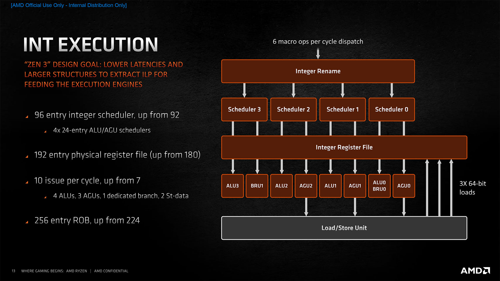
The execution engine, or combination of the integer and floating-point execution units, is the main math muscle of the CPU core. The "Zen 3" microarchitecture features improvements to both over "Zen 2." Both the INT and FP issue queues (which feed work to the two engines) have been widened and the execution window enlarged. This ensures fewer units are idle in typical programs, which increases overall performance.


AMD worked to minimize latencies at every stage of the INT execution engine, and enlarged its key structures, including the integer scheduler (96 entry vs. 92 on "Zen 2"), physical register file (192 vs. 180 on "Zen 2"), and 10 issues per cycle, up from 7 on "Zen 2." Data picker bandwidth has been significantly increased despite the same number of ALUs. The floating-point engine features the same 256-bit FPUs, but just as with the INT engine, the FP engine has latency and bandwidth improvements across the board, a faster 4-cycle FMAC, and a larger scheduler. The INT and FP improvements contribute around a fifth of the 19% overall IPC uplift.
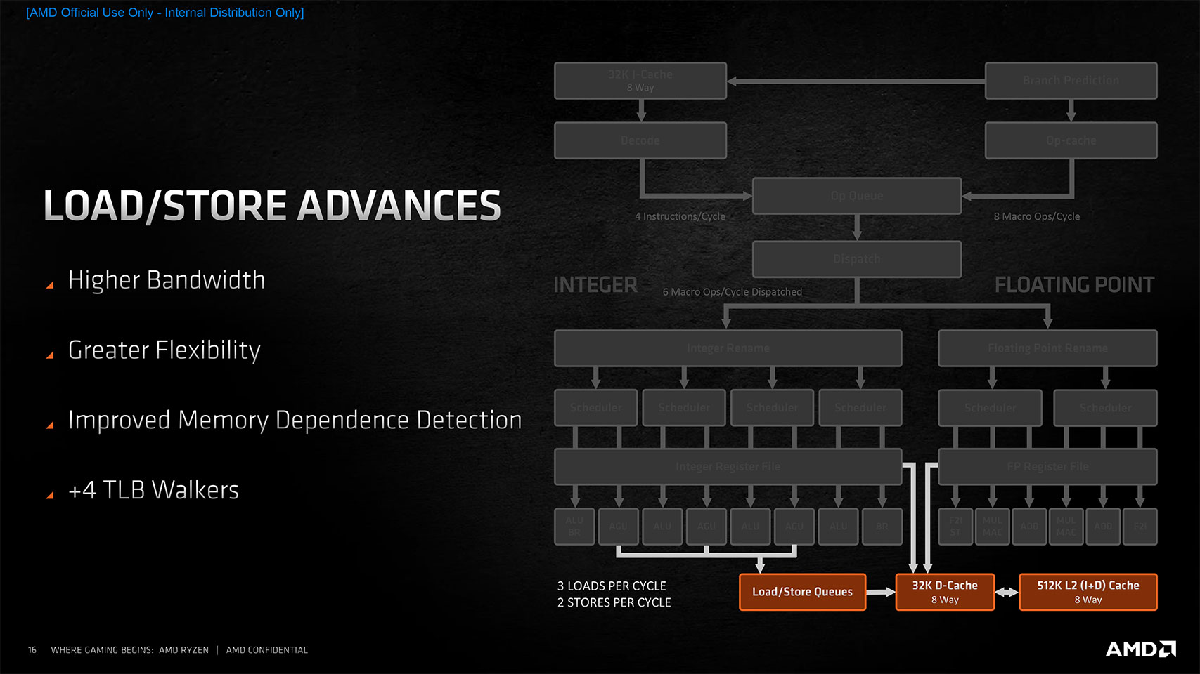
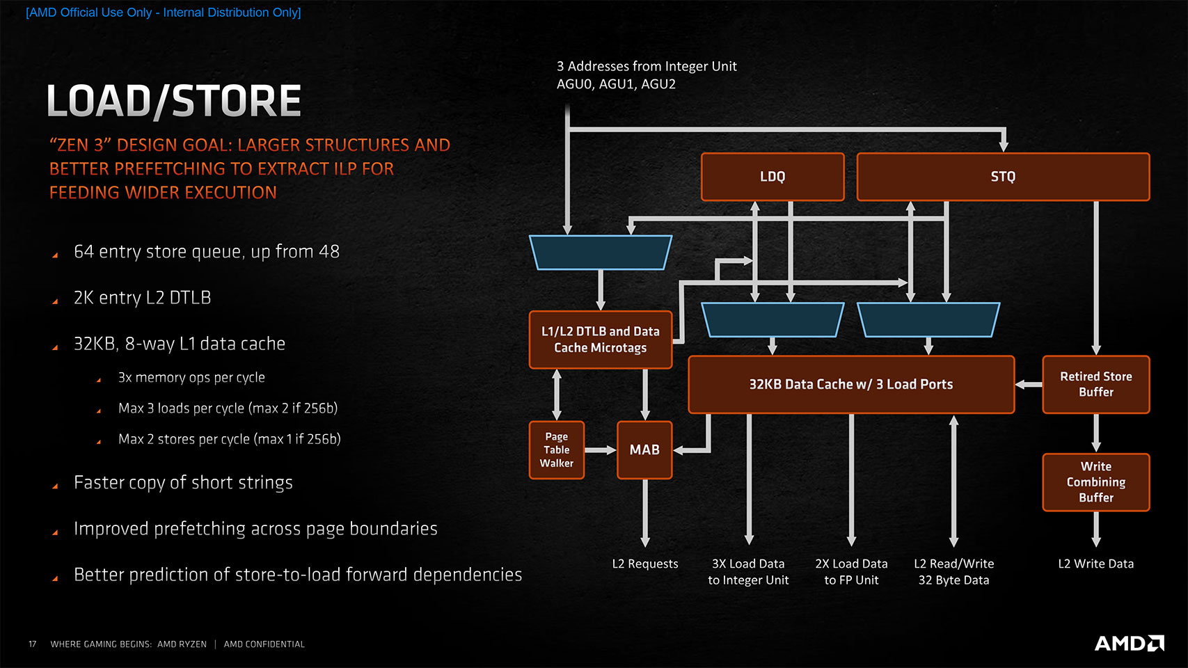
With the "Zen 3" microarchitecture, AMD addressed many bottlenecks and "intelligence" issues with the Load/Store unit. The biggest has to be bandwidth. The entry store queue has been widened to 64 from 48 on "Zen 2," and the L2 cache DTLB is 2K entries wide. The 32 KB L1 data cache has been made faster, with lower latencies. Memory dependence detection has been improved. Much like the front-end and scheduler, the load/store improvements contribute nearly a quarter of the 19% overall IPC uplift, meaning that by just optimizing the non-execution components of its core, AMD managed to pull off a vast 9% overall IPC uplift.
ISA and Security Changes
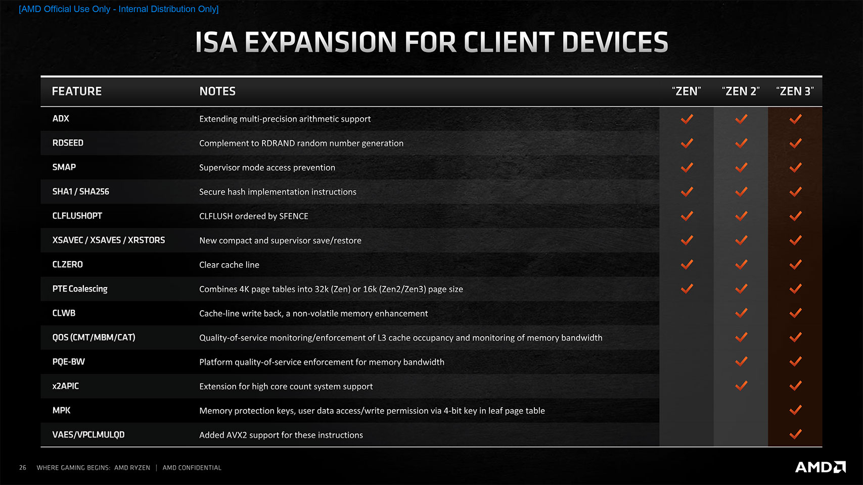
Each new microarchitecture heralds support for newer instruction sets and security hardening, and the same is the case with "Zen 3"; however, a notable absentee is AVX-512. Granted, Intel has adopted a less than perfect method of proliferating AVX-512 with certain instructions being exclusive to enterprise-segment microarchitectures and only a handful client-relevant instructions on its "Ice Lake" and "Tiger Lake" architectures, but there's no movement from AMD in this direction.
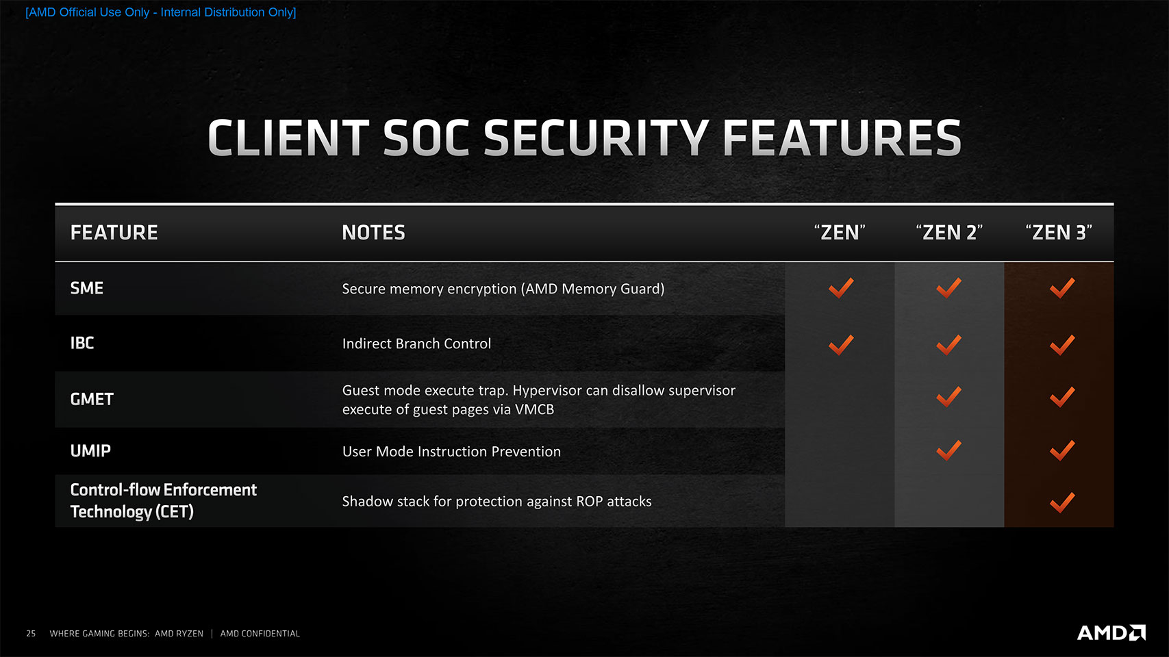
You still do get 256-bit instructions from within the AVX2 set. Also missing in action is something to rival Intel's DLBoost, which is essentially a software exposure of fixed-function hardware that accelerates matrix multiplication, in effect AI deep-learning neural net building and training. A lot of client applications, particularly image manipulation and video editing, are leveraging edge AI, and some investment from AMD on this would have been nice. That said, "Zen 3" adds two new ISA instructions, MPK (memory protection keys) and AVX2 support for AES/APCLMulQD. AMD has been ahead of Intel with CPU core security vulnerability perception, and with "Zen 3," AMD is introducing CET, or control-flow enforcement, which should provide hardening against ROP-type attacks.
Vermeer Multi-Chip Module
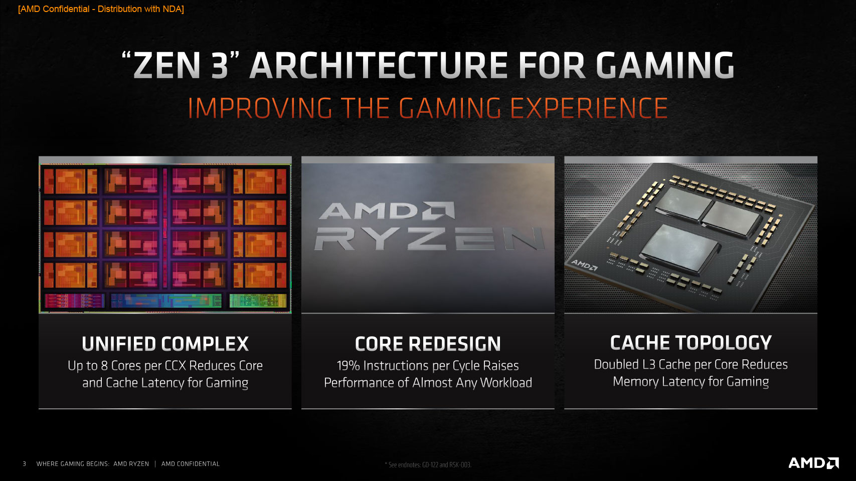
The AMD Ryzen 7 5800X "Zen 3" processor is built on a Socket AM4 multi-chip module package the company refers to as "Vermeer." Since the Ryzen 3000 "Matisse," which was the first desktop processor to implement the 7 nm silicon fabrication process, AMD figured out a way to optimize the utilization of its 7 nm foundry allocation by using two things—building only those components that tangibly benefit from the new node on 7 nm, namely the CPU cores, and moving all other components to a separate die built on older 12 nm process, the cIOD (client IO die). The CPU cores are built on tiny dies with eight cores each, which AMD refers to as the CCD (CPU core die), and on the older "Zen 2" microarchitecture, the eight cores were split into two groups of four cores, each, called CPU core complexes (CCX). Each of the two CCX on the "Zen 2" CCD had its own 16-megabyte L3 cache shared between the two cores, and communication between cores of different CCX required a round-trip to the cIOD.
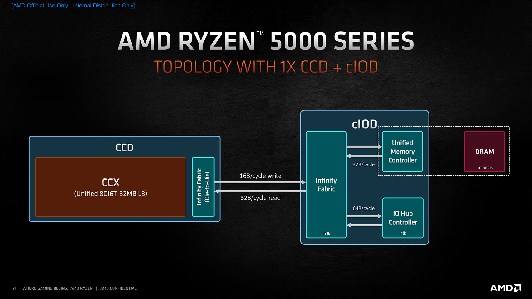
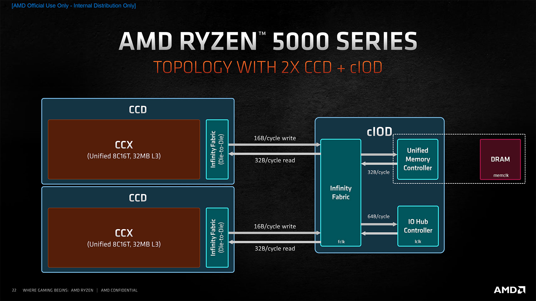
With the new "Zen 3" microarchitecture, the biggest high-level change with the CCD is AMD's enlargement of the CCX to now include up to eight cores (essentially taking up the whole CCD). There's now one 8-core CCX per CCD. The biggest dividend of this change has to be improved inter-core latency since the eight cores now share the same L3 cache; the other big dividend has to be cache size. Each core on the CCD now has access to the full 32 MB L3 as a victim cache, so lightly threaded workloads should see a performance uplift. Eight-core Ryzen 7 5000-series models, such as the 5800X, feature a single CCD with all cores enabled. 6-core parts, such as the Ryzen 5 5600X, feature one CCD with any two of the cores disabled (shouldn't matter which ones). The 12-core Ryzen 9 5900X and 16-core Ryzen 9 5950X are parts that have two 8-core CCDs besides the cIOD. The 5900X is carved out by disabling any two cores per CCD, while the 5950X has all cores enabled on both CCDs. We confirmed with AMD that Ryzen 5000 "Vermeer" uses the same exact 12 nm cIOD as the Ryzen 3000 "Matisse" with only a couple of non-physical improvements, such as improved memory clocks and clock domains.
Our Patreon Silver Supporters can read articles in single-page format.
Apr 25th, 2024 17:32 EDT
change timezone
Latest GPU Drivers
New Forum Posts
- Ubuntu 24.04 LTS released (1)
- Which new games will you be buying? (313)
- TPU's Nostalgic Hardware Club (18463)
- im new to throttelstop and i think i messed it up by copying others any hints would be very much aprreciated (2)
- Ryzen Owners Zen Garden (7243)
- What software are you using to monitor CPU temps during gaming session? (15)
- ROG Strix LC III 360 ARG AIO What should the pump speed be? (4)
- Ghetto Mods (4322)
- Legion Pro 7i, i9-13900HX. PL2 limit reason in log file (0)
- Alphacool CORE 1 CPU block - bulging with danger of splitting? (15)
Popular Reviews
- Fractal Design Terra Review
- Thermalright Phantom Spirit 120 EVO Review
- Corsair 2000D Airflow Review
- Minisforum EliteMini UM780 XTX (AMD Ryzen 7 7840HS) Review
- ASUS GeForce RTX 4090 STRIX OC Review
- NVIDIA GeForce RTX 4090 Founders Edition Review - Impressive Performance
- ASUS GeForce RTX 4090 Matrix Platinum Review - The RTX 4090 Ti
- MSI GeForce RTX 4090 Suprim X Review
- MSI GeForce RTX 4090 Gaming X Trio Review
- Gigabyte GeForce RTX 4090 Gaming OC Review
Controversial News Posts
- Sony PlayStation 5 Pro Specifications Confirmed, Console Arrives Before Holidays (116)
- Windows 11 Now Officially Adware as Microsoft Embeds Ads in the Start Menu (106)
- NVIDIA Points Intel Raptor Lake CPU Users to Get Help from Intel Amid System Instability Issues (106)
- AMD "Strix Halo" Zen 5 Mobile Processor Pictured: Chiplet-based, Uses 256-bit LPDDR5X (101)
- US Government Wants Nuclear Plants to Offload AI Data Center Expansion (98)
- AMD's RDNA 4 GPUs Could Stick with 18 Gbps GDDR6 Memory (87)
- Developers of Outpost Infinity Siege Recommend Underclocking i9-13900K and i9-14900K for Stability on Machines with RTX 4090 (85)
- Windows 10 Security Updates to Cost $61 After 2025, $427 by 2028 (84)