 340
340
AMD Ryzen 7 7800X3D Review - The Best Gaming CPU
(340 Comments) »Introduction
In this review we're testing AMD's new Ryzen 7 7800X3D, which is the company's latest gaming monster based on the 3D Vertical Cache technology. It features an 8-core Zen 4 CCD with high frequencies, and should be able to provide a generational gaming performance uplift, letting AMD surpass even the fastest of Intel's 13th Gen Core Raptor Lake processors at gaming. For the bulk of gamers and e-sports athletes that aren't big on "gaming++" workloads such as streaming, heavy video processing, and live social media; and just need a processor for maxed out AAA gaming at the highest resolutions, with the fastest graphics cards available, the 7800X3D is supposed to be their knight in shining armor.
So what exactly is it? The Ryzen 7 7800X3D in this review is an 8-core/16-thread Socket AM5 processor based on the same Zen 4 microarchitecture the company debuted its Ryzen 7000 series desktop processor family with, but featuring the 3D Vertical Cache technology that had a transformative impact on gaming performance in the previous-generation Ryzen 7 5800X3D. AMD discovered that a large cache significantly improves gaming performance, and cuts down round-trips to main memory. It hence innovated additional silicon that has 64 MB of fast SRAM cache, which is stacked on top of the CCD (CPU core complex die), and is made contiguous with the 32 MB on-die L3 cache. The CPU cores and software see a 96 MB single L3 cache.

AMD released the Ryzen 7 5800X3D around the time when its Ryzen 5000 Zen 3 series found itself bested by Intel's 12th Gen Core Alder Lake. The 5800X3D beat the fastest Core i9-12900K in gaming, forcing Intel to scamper for Special Edition chips with limited availability, such as the i9-12900KS, that level up to the 5800X3D, but at enormous power needed to maintain a 5.00 GHz all-core boost for the processor's eight P-cores. Fast forward to 2023 and we see the 7800X3D wanting to eat Intel's lunch in the high-end gaming CPU market once again, with its sights set on the Core i9-13900K.
Games don't need more than eight high-performance cores, and even Intel agrees with this notion. This is why the 5800X3D dominated the i9-12900K despite the lack of E-cores. Intel's 24-core i9-13900K only comes with eight P-cores, which handle gaming workloads. If the E-cores can get a nibble out of the processor's power-budget, they can handle background tasks. Intel is working with game developers to optimize for the Hybrid architecture and take advantage of the E-cores at a game-engine level, but so far we haven't come across a game that does this the way Intel means it. Besides, getting the E-core clusters busy would mean reduced power budget and boost-residency for the P-cores.
The sharpest critique for the 5800X3D has been that since it only has eight cores, it falls behind competing Intel processors that additionally have E-cores, in multi-threaded productivity workloads. AMD doesn't want Intel to get away making the same argument this time, and released the 16-core and 12-core 7950X3D and 7900X3D last month, which use 3D Vertical Cache on one of the two CCDs, while the other is a regular Zen 4 CCD with just 32 MB on-die cache. For non-gaming, multi-threaded productivity workloads, you get the full benefit of the high core-count, and our testing has shown the 7950X3D to present itself as a strong competitor to the i9-13900K. As a dual-CCD processor, however, there are some drawbacks, the biggest of which is to ensure that gaming workloads reside on the CCD with the 3D Vertical Cache, and there is no mis-scheduling to the other CCD. AMD released several software-based mechanisms to ensure the 7950X3D and 7900X3D work as intended. As you will see throughout this review, there's no such issue with the 7800X3D, as all its CPU cores are localized to a single CCD with 96 MB of L3 cache.
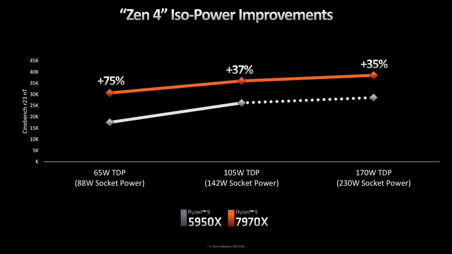
A known design drawback with 3D Vertical Cache SKUs has been that AMD adjusted power, thermals, and frequency. The 3D Vertical Cache itself operates at the same frequency as the CPU cores, so it can only be stable up to a certain frequency. AMD set the maximum boost frequency of the 7800X3D at 5.00 GHz. The overclocking options are far too limited compared to the 7700X. The T-junction max temperature is lowered, which means the processor's boosting algorithm has narrower thermal headroom in which to sustain boost frequencies. The TDP, however, is slightly increased at 120 W, compared to 105 W of the 7700X. The 5.00 GHz frequency means that the 7800X3D relies heavily on the 3D Vertical Cache feature to achieve its gaming performance targets, while non-gaming workloads which aren't memory-intensive, could actually run faster on the 7700X, which can boost up to 5.40 GHz and has a higher thermal limit.
Today's review subject, the Ryzen 7 7800X3D, costs an eye-watering $450, which puts its price higher than not just the Core i7-13700K, but also two of AMD's own 12-core SKUs, namely the 7900X and 7900. It's still significantly lower than the $580 i9-13900K, and the $750 7950X3D. In return, AMD is promising the 7800X3D to be the fastest processor for gamers to max-out their games, and pair with the fastest graphics cards out there.
| Price | Cores / Threads | Base Clock | Max. Boost | L3 Cache | TDP | Architecture | Process | Socket | |
|---|---|---|---|---|---|---|---|---|---|
| Core i5-10600K | $170 | 6 / 12 | 4.1 GHz | 4.8 GHz | 12 MB | 125 W | Comet Lake | 14 nm | LGA 1200 |
| Core i5-11600K | $200 | 6 / 12 | 3.9 GHz | 4.9 GHz | 12 MB | 125 W | Rocket Lake | 14 nm | LGA 1200 |
| Ryzen 5 5600X | $170 | 6 / 12 | 3.7 GHz | 4.6 GHz | 32 MB | 65 W | Zen 3 | 7 nm | AM4 |
| Core i5-12600K | $210 | 6+4 / 16 | 3.7 / 2.8 GHz | 4.9 / 3.6 GHz | 20 MB | 125 W | Alder Lake | 10 nm | LGA 1700 |
| Core i5-13600K | $290 | 6+8 / 20 | 3.5 / 2.6 GHz | 5.1 / 3.9 GHz | 24 MB | 125 W | Raptor Lake | 10 nm | LGA 1700 |
| Core i7-10700K | $260 | 8 / 16 | 3.8 GHz | 5.1 GHz | 16 MB | 125 W | Comet Lake | 14 nm | LGA 1200 |
| Core i7-11700K | $240 | 8 / 16 | 3.6 GHz | 5.0 GHz | 16 MB | 125 W | Rocket Lake | 14 nm | LGA 1200 |
| Ryzen 7 3700X | $200 | 8 / 16 | 3.6 GHz | 4.4 GHz | 32 MB | 65 W | Zen 2 | 7 nm | AM4 |
| Ryzen 7 5700G | $200 | 8 / 16 | 3.8 GHz | 4.6 GHz | 16 MB | 65 W | Zen 3 + Vega | 7 nm | AM4 |
| Core i7-12700K | $320 | 8+4 / 20 | 3.6 / 2.7 GHz | 5.0 / 3.8 GHz | 25 MB | 125 W | Alder Lake | 10 nm | LGA 1700 |
| Ryzen 7 5700X | $190 | 8 / 16 | 3.4 GHz | 4.6 GHz | 32 MB | 65 W | Zen 3 | 7 nm | AM4 |
| Core i7-13700K | $425 | 8+8 / 24 | 3.4 / 2.5 GHz | 5.4 / 4.2 GHz | 30 MB | 125 W | Raptor Lake | 10 nm | LGA 1700 |
| Ryzen 7 5800X | $240 | 8 / 16 | 3.8 GHz | 4.7 GHz | 32 MB | 105 W | Zen 3 | 7 nm | AM4 |
| Ryzen 7 5800X3D | $310 | 8 / 16 | 3.4 GHz | 4.5 GHz | 96 MB | 105 W | Zen 3 | 7 nm | AM4 |
| Ryzen 9 3900X | $350 | 12 / 24 | 3.8 GHz | 4.6 GHz | 64 MB | 105 W | Zen 2 | 7 nm | AM4 |
| Ryzen 5 7600 | $230 | 6 / 12 | 3.8 GHz | 5.1 GHz | 32 MB | 65 W | Zen 4 | 5 nm | AM5 |
| Ryzen 5 7600X | $245 | 6 / 12 | 4.7 GHz | 5.3 GHz | 32 MB | 105 W | Zen 4 | 5 nm | AM5 |
| Ryzen 9 5900X | $345 | 12 / 24 | 3.7 GHz | 4.8 GHz | 64 MB | 105 W | Zen 3 | 7 nm | AM4 |
| Core i9-10900K | $350 | 10 / 20 | 3.7 GHz | 5.3 GHz | 20 MB | 125 W | Comet Lake | 14 nm | LGA 1200 |
| Core i9-11900K | $350 | 8 / 16 | 3.5 GHz | 5.3 GHz | 16 MB | 125 W | Rocket Lake | 14 nm | LGA 1200 |
| Ryzen 9 5950X | $500 | 16 / 32 | 3.4 GHz | 4.9 GHz | 64 MB | 105 W | Zen 3 | 7 nm | AM4 |
| Ryzen 7 7700 | $330 | 8 / 16 | 3.8 GHz | 5.3 GHz | 32 MB | 65 W | Zen 4 | 5 nm | AM5 |
| Ryzen 7 7700X | $325 | 8 / 16 | 4.5 GHz | 5.4 GHz | 32 MB | 105 W | Zen 4 | 5 nm | AM5 |
| Core i9-12900K | $430 | 8+8 / 24 | 3.2 / 2.4 GHz | 5.2 / 3.9 GHz | 30 MB | 125 W | Alder Lake | 10 nm | LGA 1700 |
| Core i9-12900KS | $620 | 8+8 / 24 | 3.4 / 2.5 GHz | 5.5 / 4.0 GHz | 30 MB | 125 W | Alder Lake | 10 nm | LGA 1700 |
| Ryzen 7 7800X3D | $450 | 8 / 16 | 4.2 GHz | 5.0 GHz | 96 MB | 120 W | Zen 4 | 5 nm | AM5 |
| Ryzen 9 7900 | $430 | 12 / 24 | 3.7 GHz | 5.4 GHz | 64 MB | 65 W | Zen 4 | 5 nm | AM5 |
| Ryzen 9 7900X | $425 | 12 / 24 | 4.7 GHz | 5.6 GHz | 64 MB | 170 W | Zen 4 | 5 nm | AM5 |
| Ryzen 9 7900X3D | $600 | 12 / 24 | 4.4 GHz | 5.6 GHz | 128 MB | 120 W | Zen 4 | 5 nm | AM5 |
| Ryzen 9 7950X | $575 | 16 / 32 | 4.5 GHz | 5.7 GHz | 64 MB | 170 W | Zen 4 | 5 nm | AM5 |
| Ryzen 9 7950X3D | $700 | 16 / 32 | 4.2 GHz | 5.7 GHz | 128 MB | 120 W | Zen 4 | 5 nm | AM5 |
| Core i9-13900K | $570 | 8+16 / 32 | 3.0 / 2.2 GHz | 5.8 / 4.3 GHz | 36 MB | 125 W | Raptor Lake | 10 nm | LGA 1700 |
| Core i9-13900KS | $730 | 8+16 / 32 | 3.2 / 2.4 GHz | 6.0 / 4.3 GHz | 36 MB | 150 W | Raptor Lake | 10 nm | LGA 1700 |
3D Vertical Cache Technology
3D Vertical Cache is an additional 64 MB cache on a dedicated piece of silicon, which is placed on top of the region of the "Zen 4" CCD that has the 32 MB on-die L3 cache, and connected via TSVs (through-silicon vias). This cache operates at the same speed as the on-die L3 cache, and is hence designed to be contiguous to it. Software and OS see just a single 96 MB chunk of L3 cache for the CCD—it's not split into two separate chunks. Large, fast cache memory close to the logic, has been found to have a significant positive impact on gaming performance.
At a physical level, the 3D Vertical Cache is a 64 MB SRAM placed on a silicon die built on the 6 nm process; AMD refers to this die as simply the L3 Cache Die (L3D), which is stacked on top of the CPU Complex Die (CCD). Since this adds to the vertical thickness of the CCD towards its center, the edges of the CCD that have the all-important CPU cores, are layered with a highly conductive structural silicon that levels out the die. Soldered TIM then bonds the CCD with the processor's copper integrated heatspreader (IHS). While the 7950X3D and 7900X3D are dual-CCD (dual-chiplet) processors that have to deal with getting the OS scheduling just right for games to benefit from 3DV cache, the 7800X3D in this review is a single-CCD processor, and has no such issues.
The Zen 4 Platform

AMD Zen has been one of the most remarkable turnarounds for a company in the semiconductor industry, and has had a profound impact on the consumer, as it influenced Intel's CPU core-counts. With each new generation of Zen, AMD delivered IPC and overall performance improvements, and Zen 4 stands out as it not only aims to improve performance, but also introduce a brand-new platform after five years of Socket AM4. As a parting gift, AMD enabled official Zen 3 support on even the oldest 300-series chipset, going to show just how consumer-friendly AM4 was, something the company hopes to repeat with AM5. The new AM5 socket was needed as the company enables the latest I/O, including DDR5 memory and PCI-Express Gen 5, besides power-delivery improvements. The socket can now deliver up to 230 W of power, which gives AMD room to increase CPU core-counts in the future. AM5 is a land-grid array, just like Intel desktop sockets, but the company retained CPU cooler compatibility with AM4.
Zen 4 Chip Configuration
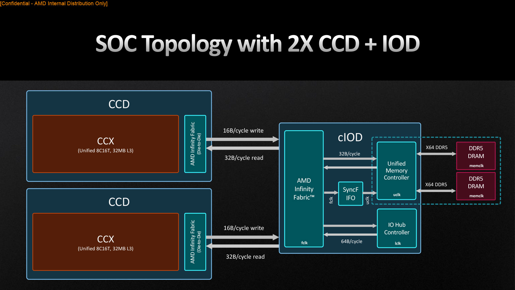
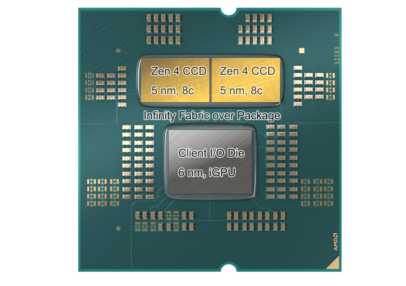
The Ryzen 7000 series desktop processor, codenamed "Raphael," is a multi-chip module, just like the Ryzen 5000 "Vermeer" and Ryzen 3000 "Matisse." The CPU cores are located in specialized dies called CCDs (CPU complex dies), while the platform I/O control is located in a separate die called cIOD (client I/O die). The CCDs were fabricated on the latest TSMC 5 nm EUV (N5) node, while the cIOD are done so on TSMC 6 nm (N6) nodes. The idea here is that the parts that benefit the most from the switch to the latest foundry process—the CPU cores—are built on this node; while everything else that can do with a slightly older node, uses that instead. This way AMD can make the most of its 5 nm foundry allocation with TSMC. The MCM contains a cIOD, and two 8-core CCDs in case of the Ryzen 9 7950X and 7900X; or one 8-core CCD in case of the Ryzen 7 7700X and Ryzen 5 7600X. Infinity Fabric interconnect handles communications not just within these dies, but also between them. The transition to fast DDR5 memory and PCIe Gen 5 means that AMD now can push instructions and data around faster. It did so with microarchitectural improvements to the "Zen 4" core itself, while also increasing the Infinity Fabric bandwidth between the cores.
The Zen 4 CPU Core
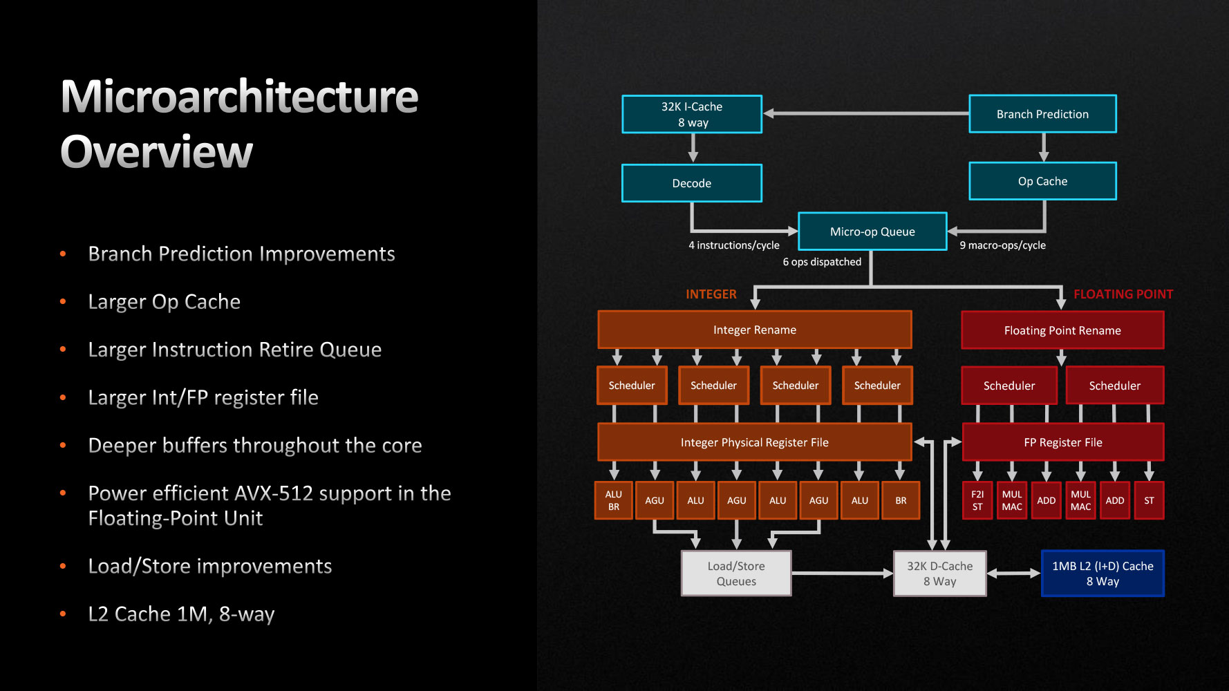
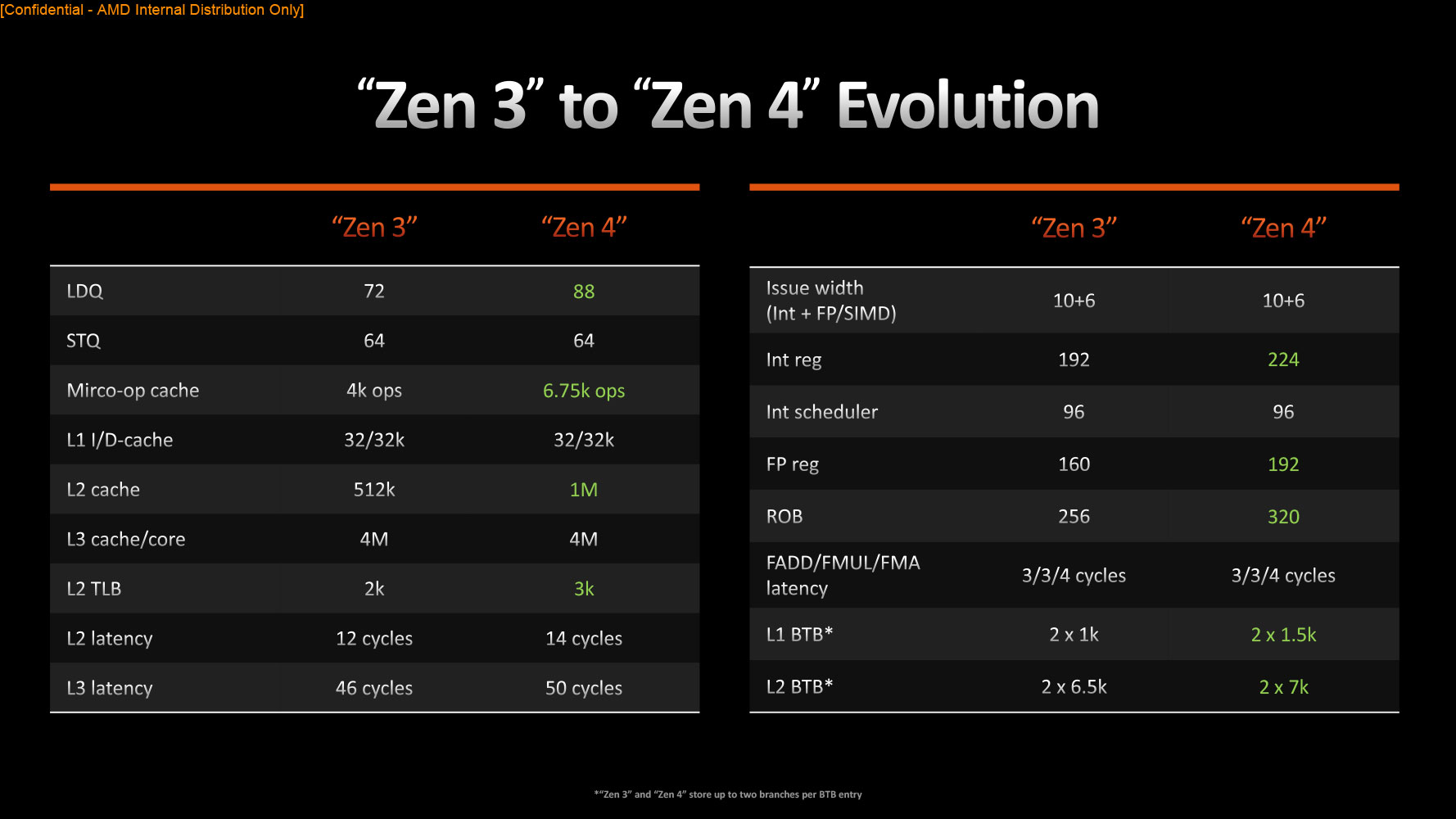
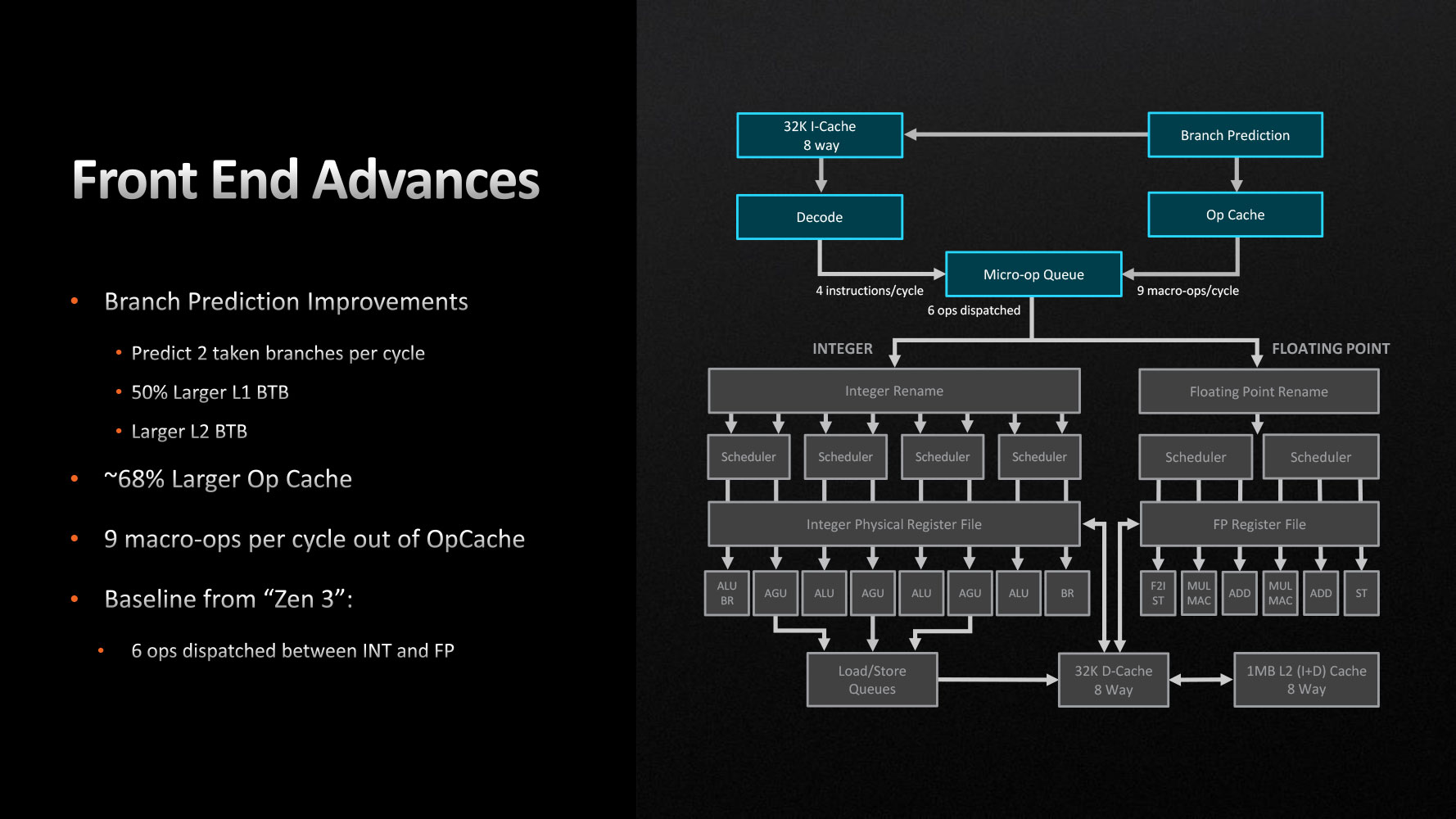
All cores in Ryzen 7000 series processors are of the same kind, what Intel would consider a performance-core, or P-core. AMD has worked on all three key stages of the CPU—the front-end, the execution, and the load/store. The front-end is the "mouth" of the CPU core, and prepares data and instructions for execution. Front-end improvements begin at the Branch Prediction unit, which can how predict 2 taken branches per clock-cycle, and comes with larger L1 and L2 branch-target buffers (BTBs). AMD had for the very first time introduced an OpCache with Zen, improving it over time. AMD has increased the size of the OpCache by around 68 percent. It can now handle 9 macro-ops per cycle. The micro-op queue dispatch rate to the execution stage is still 6.
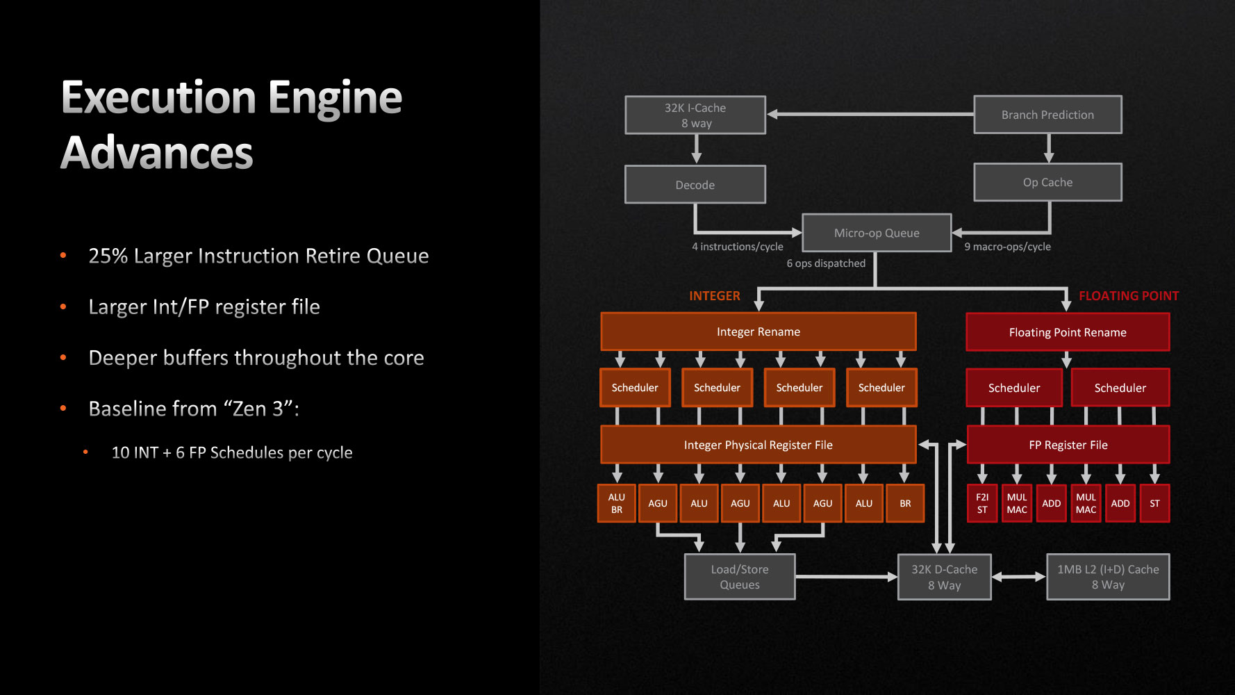
The Execution Stage is the main number-crunching machinery, and broadly features two components for the kind of math workload being executed—Integer and Floating Point. The "Zen 4" execution stage features a 25% larger instruction retire queue, larger register files, and higher buffer queue-depths throughout the core.

With "Zen 4," AMD is introducing support for AVX-512, in a bid to increase the processor's AI inferencing performance. The company did this in a die-area efficient, and energy-efficient manner, with no impact on CPU core frequency. AVX-512 operations are executed on a dual-pumped 256-bit FPU, rather than building ground-up 512-bit FP machinery. VNNI and Bfloat16 instruction-sets are also added, which mean that "Zen 4" can handle pretty much all of the AVX-512 client-relevant workloads that competing Intel processors can.


The Load/Store unit is the part of the core that interfaces with the memory sub-system. The "Zen 4" core gets a 22 percent larger Load Queue, with improved data-port conflict-resolution. There's a 50% larger L2 data transition lookaside buffer. The cache-hierarchy of the Ryzen 7000 desktop processor is similar to that of Ryzen 5000, with a few key differences, besides bandwidth/latency improvements—the dedicated L2 cache has been doubled in size to 1 MB per core. The eight CPU cores on a CCD share a monolithic 32 MB L3 cache, with uniform access to each core.
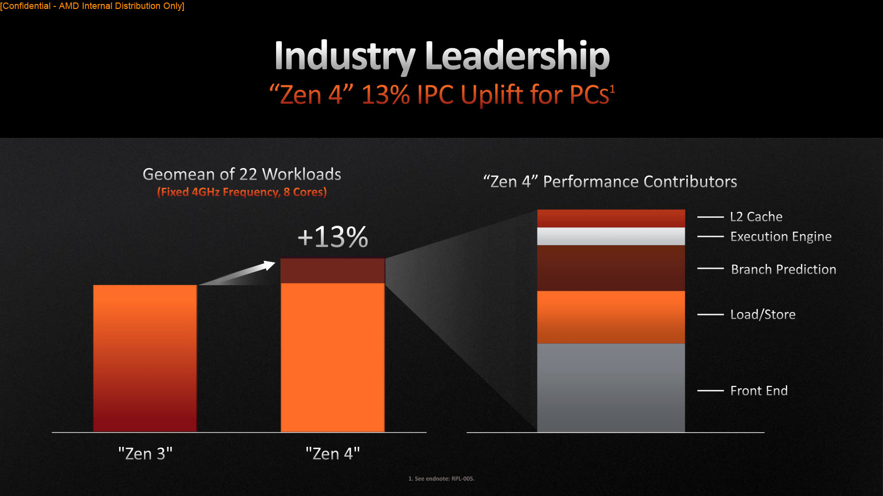
These improvements contribute to a 13 percent IPC improvement over "Zen 3," AMD claims. The company provided a break-up of which components are contributing to the IPC uplift, and we see that close to two-thirds of it are coming from improvements to the front-end and load/store stages. Branch prediction improvements contribute a fifth of this uplift. Interestingly, the L2 cache contributes barely 1/10th of the IPC uplift, in the tested applications—we believe this increase is mostly relevant for server applications where it should be able to make a difference. Intel's "Golden Cove" P-core comes with 1.25 MB L2 cache, and "Raptor Cove" features 2 MB. Despite the doubling in L2 cache sizes, the resulting increase in cache latency is very well contained (from 12 cycles on the 512 KB L2 of "Zen 3," to just 14 cycles on "Zen 4").
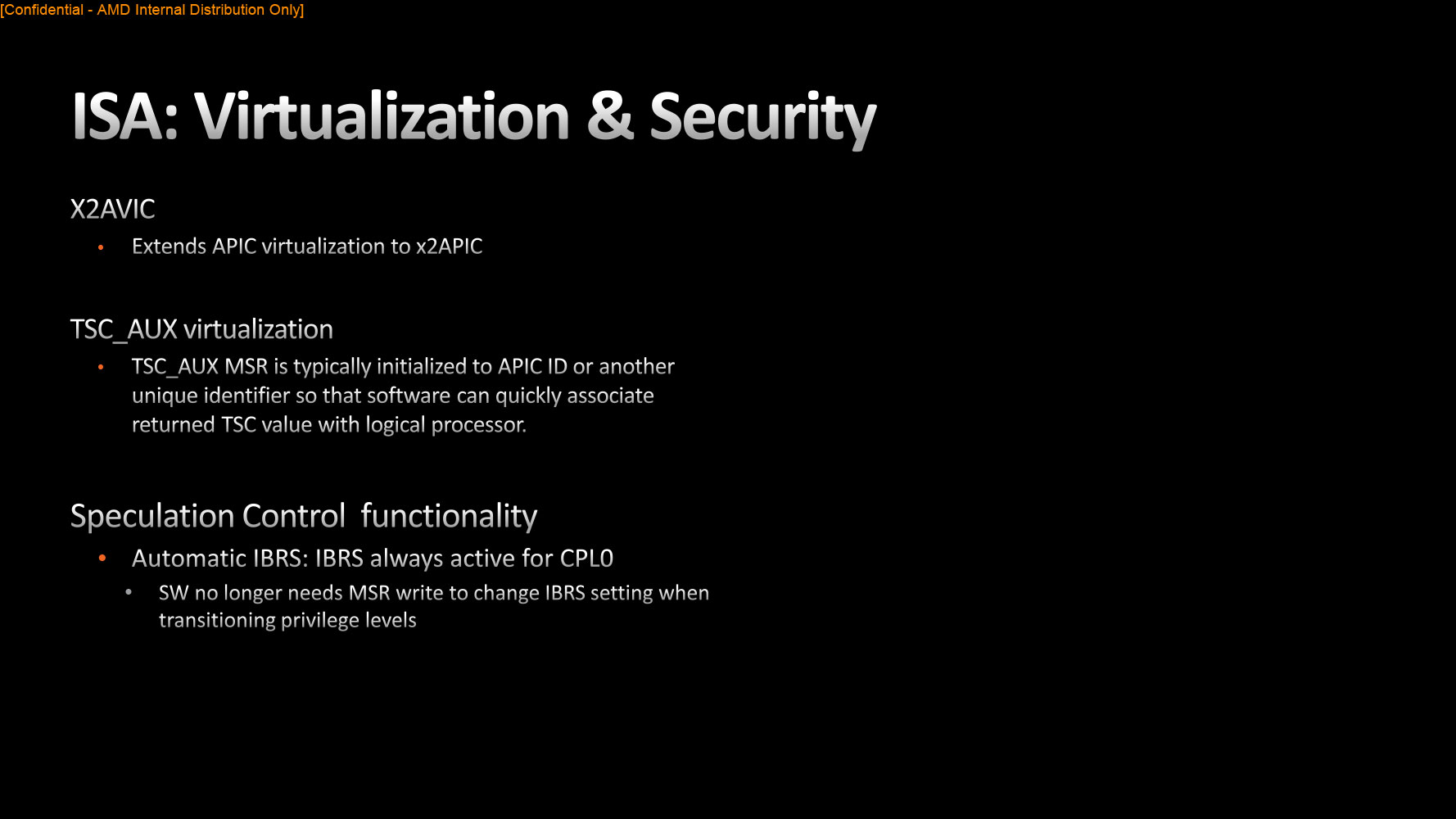
VBS (virtualization-based security) is the standard on new Windows 11 installs and gets activated automatically, unless you specifically disable it. Windows 11 Security Center already flags VBS not being enabled as a warning, similar to Antivirus being disabled or outdated. AMD made several improvements to the Virtualization feature-set, to reduce its performance impact in a VBS-enabled client environment. This includes speculation control, dual AVIC to go with the physical dual-APIC, and TSC_AUX virtualization.
New 6 nm IO Die

Ryzen 3000 "Matisse" and Ryzen 5000 "Vermeer" processors featured a cIOD built on the 12 nm FinFET Global Foundries node, but with Ryzen 7000 "Raphael," AMD is taking a giant leap toward improving the power characteristics of the cIOD, by building it on the new 6 nm TSMC node. This was needed mainly because the cIOD now packs an RDNA2 iGPU, besides the higher bandwidth switching fabric of the DDR5 and PCIe Gen 5 interfaces also warranting the change. The 12 nm previous-gen cIOD TDP was already estimated to be up to 15 W, and the addition of an iGPU would've thrown things off gear. In addition to 6 nm, AMD is deploying several of the power-management features of the Ryzen 6000-series "Rembrandt" mobile processor on this cIOD, which mainly have to do with aggressive power management and rapid sleep/wake for the various components on the die.
The new 6 nm cIOD packs a dual-channel DDR5 memory controller (4x 40-bit channels, including ECC and hardware-accelerated encryption support), with native support for DDR5-5200; a PCI-Express 5.0 x28 root-complex; a USB 3.2 controller with support for 20 Gbps 2x2 ports, USB-C, and DisplayPort passthrough from the iGPU. AMD was very clear that the inclusion of an iGPU doesn't make "Raphael" an APU, because the iGPU is rather basic, just about enough for non-gaming workloads. The company intends to continue making APUs—processors with beefy iGPUs for mainstream gaming performance—including for the desktop platform. Full ECC support on desktop is technically possible, but it will depend on the motherboard manufacturers—AMD isn't doing anything to prevent them from making their boards ECC compatible.

The Radeon 610 iGPU is based on the RDNA2 graphics architecture, and packs just two Compute Units, which work out to 128 stream processors. The Display CoreNext (DCN) and Video CoreNext (VCN) components are of modern design. The VCN offers hardware-accelerated AV1 and H.265 decode, as well as hardware-accelerated H.265 encode. Just to clarify, there is hardware AV1 decode support, but no encode, which isn't a big deal at all. In terms of monitors, the DCN supports DisplayPort 2.0 UHBR10, HDMI 2.1 with FRL, and DisplayPort passthrough for the USB type-C ports connected to the on-die USB 3.2 controller. When paired with a discrete graphics card on Windows 10 or Windows 11, the iGPU supports Hybrid graphics, much in the same way as it's implemented on notebooks. You plug in your monitor to the iGPU, and it wakes up your discrete GPU (graphics card) when needed. The RDNA2 compute units are of the same kind you'd find in Radeon RX 6000 series GPUs, including ray tracing support, but this is of no use on the Radeon 610. The only reason AMD went with RDNA2 is because it can offer comparable levels of performance with just two CUs, to a "Vega" based iGPU that would need more CUs (thereby increasing die-size).

As we mentioned earlier, AMD needed a new socket as it was transitioning to DDR5 and PCIe Gen 5, which come with stiff physical-layer signaling requirements that AM4 couldn't provide. AM5 also makes processors "future-ready" as it enables two-way communication with the voltage regulators. The added pin-count was needed not just for DDR5 and its 40-bit sub-channels, but also for four additional PCIe lanes. The processor puts out a total of 28 PCIe Gen 5 lanes. 16 of these are meant for PEG (graphics card slots); 4 serve as chipset bus, and 8 lanes are available for the motherboard vendors to play around with: either wiring them both out as M.2 Gen 5 x4 slots, or wire one of them as M.2, and use the remaining 4 lanes for high-bandwidth devices, such as discrete USB4 controllers, 80 Gbps Thunderbolt 4 controllers, or even CPU-attached low-latency network interfaces. AM5 also significantly increases power-delivery capability over AM4—up to 230 W. The increased power should enable the "Zen 4" cores to run at very high clock-speeds approaching the 6 GHz-mark, or in the future, even enable core-count increases.
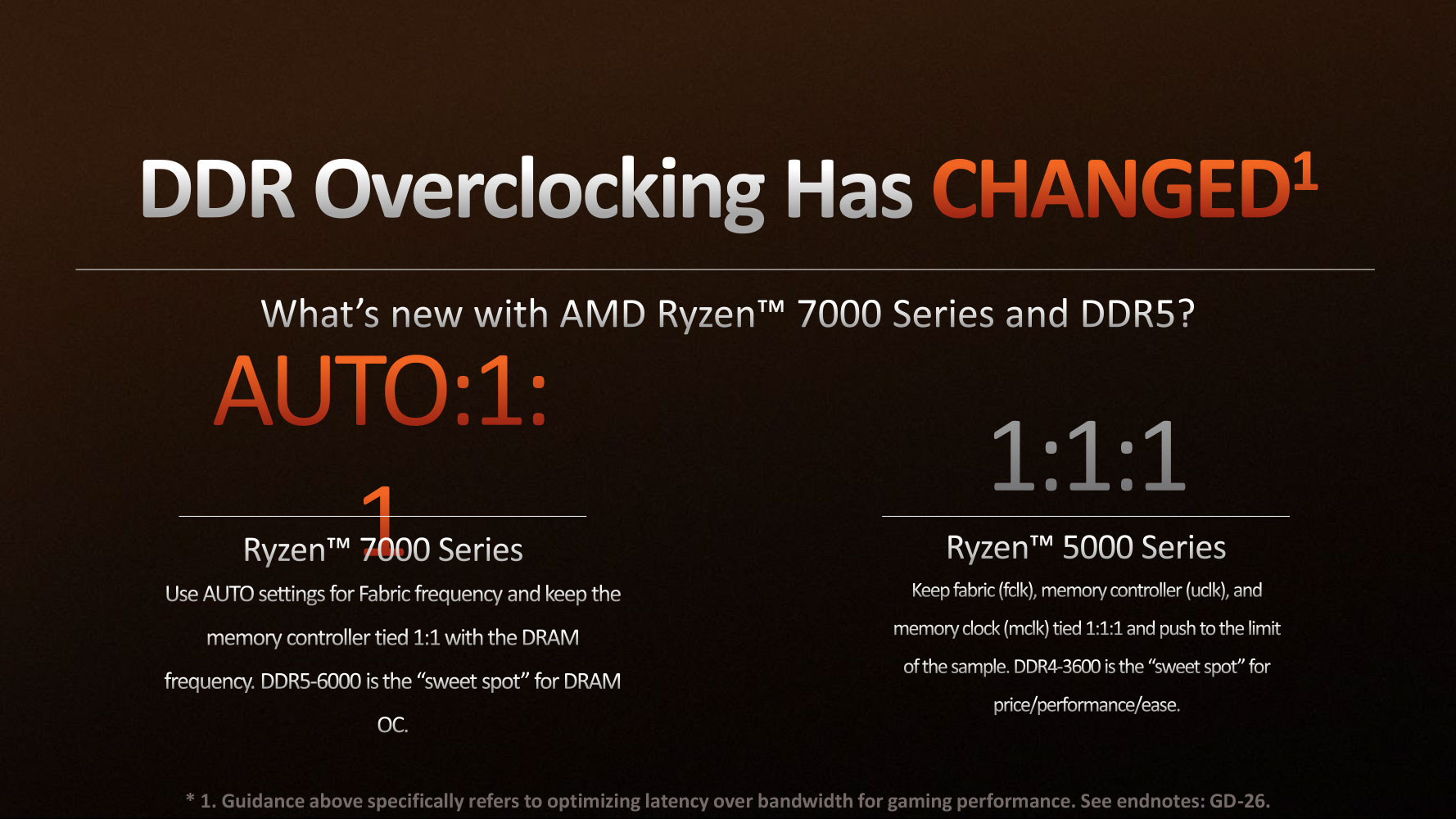
The clock-domains of Ryzen 7000 are similar to those of the Ryzen 5000 series. FCLK defines the Infinity Fabric clock-speed, which is de-linked from UCLK (memory controller clock), and MCLK (DRAM clock). AMD says that DDR5-6000 strikes the "sweetspot" in that this is the highest MCLK you can run while retaining certain memory overclocker optimizations. On Zen 3 you'd want to run Infinity Fabric in sync with memory, but this isn't possible anymore, because FCLK can't reach 3000 MHz (assuming DDR5-6000 memory). Now the optimum config is to run FCLK at 2000, basically a 3:2 divider. Picking "auto" in the BIOS will automatically aim for that setting. Above 6000 MHz, the strategy will be changed to 2:1 ratio.
AMD X670E, B650E, and A620 Chipsets
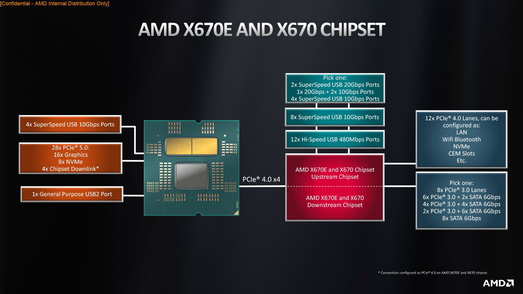

AMD took a unique approach to chipsets with this generation. The top-tier chipset now comes in two flavors, X670E and X670. Both are identical in downstream I/O, but the X670E offers PCIe Gen 5 PEG besides CPU-attached Gen 5 NVMe; whereas the X670 only offers Gen 5 on the CPU-attached M.2 NVMe slot, but not PEG (which is Gen 4). A similar approach is taken when segregating the mid-tier B650E from the B650. The lack of Gen 5 PEG should significantly reduce motherboard costs, as designers would be saving on both Gen 5 re-drivers and the steep wiring requirements to avoid signal-corruption.
X670E is a 2-chip chipset unlike the previous-gen X570. This was done to increase the downstream PCIe connectivity. The chipset now offers up to 12x PCIe Gen 4 and up to 8x PCIe Gen 3 downstream lanes (not counting the lanes from the CPU). This lets motherboard designers wire out three additional M.2 Gen 4 slots attached to the chipset, while the Gen 3 lanes handle low-bandwidth onboard devices. AMD adopted a wacky way to connect the two bridges that make up the chipset. There is an "upstream" chipset that's wired to the AM5 SoC over a PCI-Express 4.0 x4 connection; the second bridge is called "downstream" chipset, and is connected to four of the PCIe Gen 4 downstream lanes of the "upstream" chipset. The X670/E puts out up to two 20 Gbps USB 3.2, up to eight 10 Gbps USB 3.2, and twelve USB 2.0. The B650E and B650 look like more reasonable single-chip chipsets. They talk to the SoC over PCI-Express 4.0 x4, and wire out 8x PCIe Gen 4 downstream lanes, and up to 4x PCIe Gen 3 downstream lanes. You get half the number of USB SuperSpeed ports as the X670/E.

In early April 2023, AMD introduced the cost-effective A620 chipset. This makes sub-$100 motherboards possible, but is intended for 65 W Ryzen 7000 processors. Some motherboard vendors may choose to provide support for 7000X and 7000X3D processors, but their processor power limits could be impacted. The A620 is similar in connectivity to the B650 (non-E), but you are limited to PCIe Gen 4 for both the PEG and CPU-attached NVMe slots, and the downstream PCIe connectivity from the chipset is limited to Gen 3. CPU overclocking is completely disabled, but you can overclock the memory, and enable EXPO profiles just fine.
AMD EXPO Memory


With Ryzen 7000 series, AMD is introducing EXPO (extended profiles for overclocking); a feature that's identical in concept to Intel XMP. AMD EXPO-certified DDR5 modules come with an easy method of applying the advertised memory speeds and timings—you simply select a toggle in the opening screen of your motherboard's UEFI BIOS program. EXPO differs from XMP in that it includes fine settings that are unique to the AMD architecture, and it's also an open standard. Until now, XMP modules installed on AMD systems relied either on painstaking manual overclocking, or use of DOCP, a feature that attempts to translate the settings in the XMP profile to "nearest neighbors" of AMD-compatible settings. This was sub-optimal. EXPO is royalty-free compared to XMP, so any memory manufacturer can implement it for free. Ryzen 7000 can run any PC-DDR5 memory in the market, including XMP-certified ones, so don't fret if you can't find EXPO kits just yet.
Socket AM5


Here are a few pictures of Socket AM5, the star-attraction with this platform. This is a land-grid array (LGA) socket with 1,718 pins.


As with every LGA socket, the pins are on the motherboard, whereas the processor package has contacts that interface with those pins, while a retention brace holds the package in place with a locking lever. Installing a processor on AM5 is similar to doing so on any of the dozens of Intel LGA sockets.


On Socket AM4, removing the four mounting screws resulted in the backplate falling off, which meant you needed three hands when installing a cooler, and several vendors also bundled their own backplates. On Socket AM5 the backplate isn't designed to be removed, which makes cooler installation MUCH easier.

The caps for the socket are not identical to the Intel LGA sockets, so you can't reuse them.
Our Patreon Silver Supporters can read articles in single-page format.
May 5th, 2024 21:37 EDT
change timezone
Latest GPU Drivers
New Forum Posts
- What software are you using to monitor CPU temps during gaming session? (21)
- Apparently Valve is giving refunds on Helldivers 2 regardless of hour count. Details inside. (74)
- Overheating/undervolt/setup issues (2)
- Only some humans can see refresh rates faster than others, I am one of those humans. (138)
- Alphacool CORE 1 CPU block - bulging with danger of splitting? (101)
- Current Sales, Bundles, Giveaways (10227)
- FINAL FANTASY XIV: Dawntrail Official Benchmark (84)
- The Official Thermal Interface Material thread (1157)
- Random black screen - GPU or PSU bricked? (9)
- Benchmarking Unity graphics performance in WebGL (42)
Popular Reviews
- Finalmouse UltralightX Review
- ASRock NUC BOX-155H (Intel Core Ultra 7 155H) Review
- Meze Audio LIRIC 2nd Generation Closed-Back Headphones Review
- Cougar Hotrod Royal Gaming Chair Review
- Upcoming Hardware Launches 2023 (Updated Feb 2024)
- Montech Sky Two GX Review
- AMD Ryzen 7 7800X3D Review - The Best Gaming CPU
- HYTE THICC Q60 240 mm AIO Review
- ASUS Radeon RX 7900 GRE TUF OC Review
- Logitech G Pro X Superlight 2 Review - Updated with 4000 Hz Tested
Controversial News Posts
- Intel Statement on Stability Issues: "Motherboard Makers to Blame" (240)
- Windows 11 Now Officially Adware as Microsoft Embeds Ads in the Start Menu (167)
- AMD to Redesign Ray Tracing Hardware on RDNA 4 (154)
- Sony PlayStation 5 Pro Specifications Confirmed, Console Arrives Before Holidays (117)
- AMD's RDNA 4 GPUs Could Stick with 18 Gbps GDDR6 Memory (114)
- NVIDIA Points Intel Raptor Lake CPU Users to Get Help from Intel Amid System Instability Issues (106)
- AMD Ryzen 9 7900X3D Now at a Mouth-watering $329 (104)
- AMD "Strix Halo" Zen 5 Mobile Processor Pictured: Chiplet-based, Uses 256-bit LPDDR5X (103)