 387
387
AMD Ryzen 9 7950X3D Review - Best of Both Worlds
(387 Comments) »Introduction
The Ryzen 9 7950X3D review is here, AMD is ready to take on Intel's mighty Raptor Lake. Bringing the latest upgrades to the Ryzen 7000 "Zen 4" family, this processor rocks 3D Vertical Cache technology along with a massive 16-core/32-thread count, and its makers claim that it levels up to the Core i9-13900K both in gaming and multi-threaded productivity, making it the most powerful desktop processor you can buy from the AMD camp. The best part? It's being launched at the same $700 MSRP as the standard 7950X, which is now $50-75 cheaper in the market; and remains drop-in compatible with Socket AM5 motherboards, although using the latest BIOS and drivers is required.
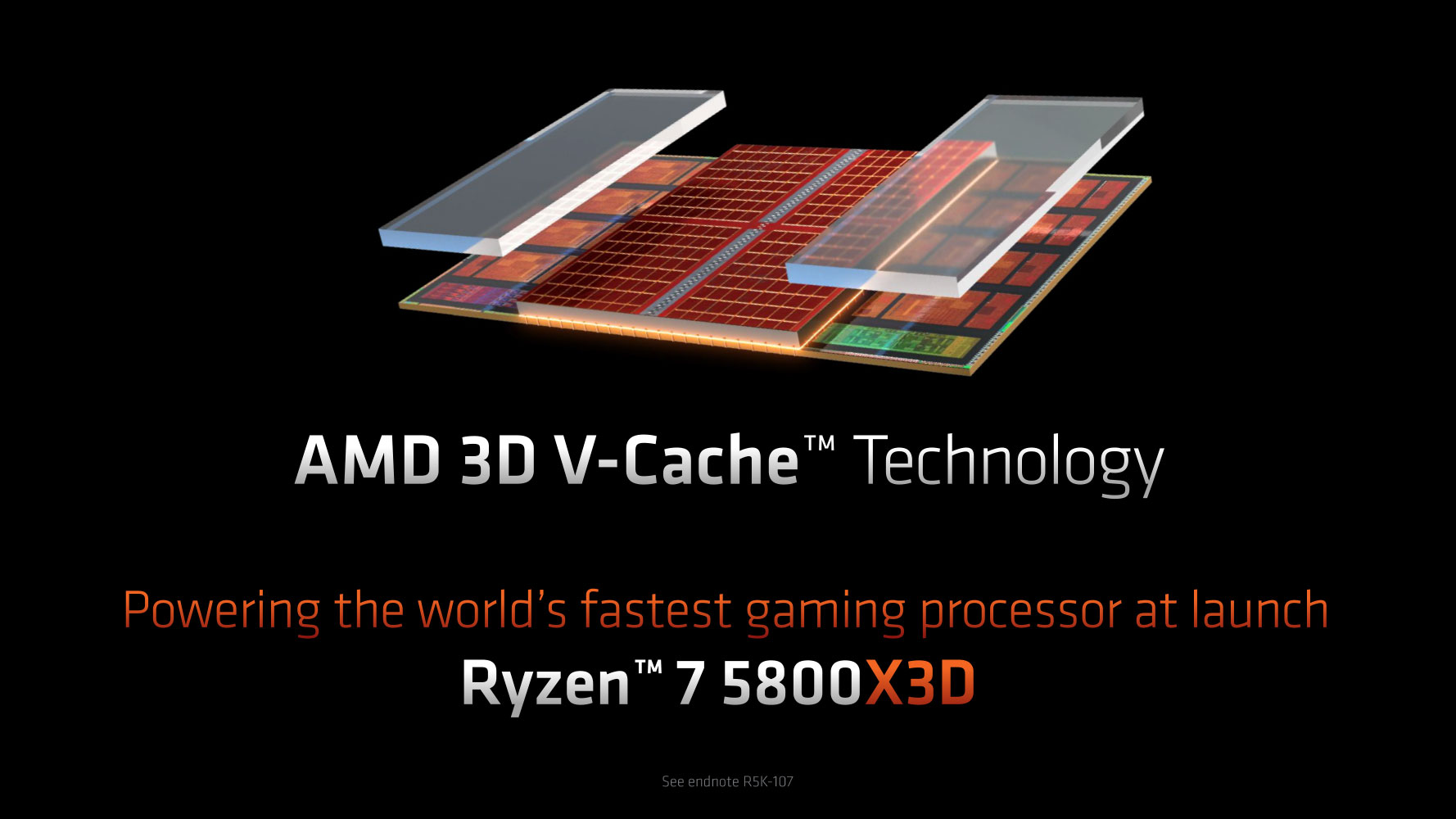
The 3D Vertical Cache technology proved its mettle with the Ryzen 7 5800X3D 8-core/16-thread processor AMD launched in 2022, where it elevated the processor's gaming performance to match that of the fastest Intel processor of the time, the i9-12900K "Alder Lake," despite being based on the generationally older "Zen 3" architecture. While the "Zen 4" architecture matches "Alder Lake" on its own, without 3D Vertical Cache, it was found falling short of "Raptor Lake" in gaming. All eyes are now on 3D Vertical Cache to work its magic again, to bring "Zen 4" into the same league as "Raptor Lake," so you're once again spoiled for choice between the two brands. While the older 5800X3D matched the i9-12900K in gaming, its lower CPU core-count meant that the "Alder Lake" zoomed past in multi-threaded productivity. This time around, AMD isn't in the mood to compromise on core-counts, and brings 3D Vertical Cache to 16-core, 12-core and 8-core Ryzen 7000X3D-series models.

The 3D Vertical Cache is a 64 MB fast SRAM cache that's stacked on top of the "Zen 4" CCD (CPU complex die), over the region of the die that has the on-die 32 MB L3 cache. This 6 nm die, called simply the L3D (L3 cache die), expands the L3 cache available to the 8 CPU cores on that CCD, from 32 MB to 96 MB. It's contiguous with the on-die L3 cache, and operates at the same speed. The vast 96 MB of last-level cache has a profound impact on gaming performance, as was proven with the 5800X3D reviews.
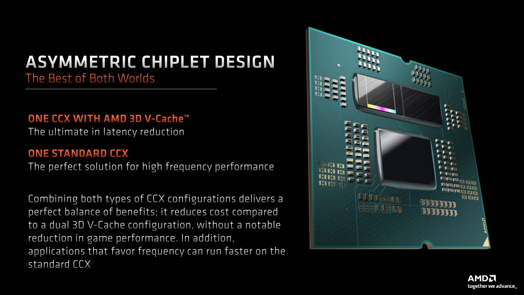
There's only one catch, though. The Ryzen 9 7950X3D is a 16-core processor, which means it has two 8-core CCDs. It turns out that one of the two is a regular "Zen 4" CCD with just 32 MB on-die L3 cache, like the one found in the 7950X. AMD's explanation for this design-choice is rather complex: it saves on cost, given that games need no more than 8 CPU cores (as is reaffirmed by Intel's decision to give its desktop processors no more than 8 performance-cores); and that the second CCD that's unsaddled with stacked cache is free to boost to higher frequencies. We'll explain more on how this works later in this review.
The Ryzen 9 7950X3D has all the goodies Socket AM5 brings to the table, including PCI-Express Gen 5 for not just the main PCIe slot, but also a CPU-attached NVMe SSD without eating into the x16 lanes (something that's lacking on the current Intel platform); and support for the latest DDR5 memory. There is, however, no DDR4 memory support, and motherboard prices are just as steep as Intel, so your price for entry into this platform is slightly higher compared to Intel, where you have the option of using cheaper DDR4 memory and motherboards. We take the AMD Ryzen 9 7950X3D for a spin through a vast new selection of gaming and productivity benchmarks to tell you if AMD is back on the top.
| Price | Cores / Threads | Base Clock | Max. Boost | L3 Cache | TDP | Architecture | Process | Socket | |
|---|---|---|---|---|---|---|---|---|---|
| Ryzen 7 5800X | $240 | 8 / 16 | 3.8 GHz | 4.7 GHz | 32 MB | 105 W | Zen 3 | 7 nm | AM4 |
| Ryzen 7 5800X3D | $310 | 8 / 16 | 3.4 GHz | 4.5 GHz | 96 MB | 105 W | Zen 3 | 7 nm | AM4 |
| Ryzen 9 3900X | $350 | 12 / 24 | 3.8 GHz | 4.6 GHz | 64 MB | 105 W | Zen 2 | 7 nm | AM4 |
| Ryzen 5 7600 | $230 | 6 / 12 | 3.8 GHz | 5.1 GHz | 32 MB | 105 W | Zen 4 | 5 nm | AM5 |
| Ryzen 5 7600X | $245 | 6 / 12 | 4.7 GHz | 5.3 GHz | 32 MB | 105 W | Zen 4 | 5 nm | AM5 |
| Ryzen 9 5900X | $345 | 12 / 24 | 3.7 GHz | 4.8 GHz | 64 MB | 105 W | Zen 3 | 7 nm | AM4 |
| Core i9-10900K | $350 | 10 / 20 | 3.7 GHz | 5.3 GHz | 20 MB | 125 W | Comet Lake | 14 nm | LGA 1200 |
| Core i9-11900K | $350 | 8 / 16 | 3.5 GHz | 5.3 GHz | 16 MB | 125 W | Rocket Lake | 14 nm | LGA 1200 |
| Ryzen 9 5950X | $500 | 16 / 32 | 3.4 GHz | 4.9 GHz | 64 MB | 105 W | Zen 3 | 7 nm | AM4 |
| Ryzen 7 7700 | $330 | 8 / 16 | 3.8 GHz | 5.3 GHz | 32 MB | 65 W | Zen 4 | 5 nm | AM5 |
| Ryzen 7 7700X | $325 | 8 / 16 | 4.5 GHz | 5.4 GHz | 32 MB | 105 W | Zen 4 | 5 nm | AM5 |
| Core i9-12900K | $430 | 8+8 / 24 | 3.2 / 2.4 GHz | 5.2 / 3.9 GHz | 30 MB | 125 W | Alder Lake | 10 nm | LGA 1700 |
| Core i9-12900KS | $620 | 8+8 / 24 | 3.4 / 2.5 GHz | 5.5 / 4.0 GHz | 30 MB | 125 W | Alder Lake | 10 nm | LGA 1700 |
| Ryzen 7 7800X3D | $450 | 8 / 16 | 4.2 GHz | 5.0 GHz | 96 MB | 120 W | Zen 4 | 5 nm | AM5 |
| Ryzen 9 7900 | $430 | 12 / 24 | 3.7 GHz | 5.4 GHz | 64 MB | 65 W | Zen 4 | 5 nm | AM5 |
| Ryzen 9 7900X | $440 | 12 / 24 | 4.7 GHz | 5.6 GHz | 64 MB | 170 W | Zen 4 | 5 nm | AM5 |
| Ryzen 9 7900X3D | $600 | 12 / 24 | 4.4 GHz | 5.6 GHz | 128 MB | 120 W | Zen 4 | 5 nm | AM5 |
| Ryzen 9 7950X | $590 | 16 / 32 | 4.5 GHz | 5.7 GHz | 64 MB | 170 W | Zen 4 | 5 nm | AM5 |
| Ryzen 9 7950X3D | $700 | 16 / 32 | 4.2 GHz | 5.7 GHz | 128 MB | 120 W | Zen 4 | 5 nm | AM5 |
| Core i9-13900K | $570 | 8+16 / 32 | 3.0 / 2.2 GHz | 5.8 / 4.3 GHz | 36 MB | 125 W | Raptor Lake | 10 nm | LGA 1700 |
| Core i9-13900KS | $730 | 8+16 / 32 | 3.2 / 2.4 GHz | 6.0 / 4.3 GHz | 36 MB | 150 W | Raptor Lake | 10 nm | LGA 1700 |
3D Vertical Cache Technology
3D Vertical Cache is an additional 64 MB cache on a dedicated piece of silicon, which is placed on top of the region of the "Zen 4" CCD that has the 32 MB on-die L3 cache, and connected via TSVs (through-silicon vias). This cache operates at the same speed as the on-die L3 cache, and is hence designed to be contiguous to it. Software and OS see just a single 96 MB chunk of L3 cache for the CCD—it's not split into two separate chunks. Large, fast cache memory close to the logic, has been found to have a significant positive impact on gaming performance.
At a physical level, the 3D Vertical Cache is a 64 MB SRAM placed on a silicon die built on the 6 nm process; AMD refers to this die as simply the L3 Cache Die (L3D), which is stacked on top of the CPU Complex Die (CCD). Since this adds to the vertical thickness of the CCD towards its center, the edges of the CCD that have the all-important CPU cores, are layered with a highly conductive structural silicon that levels out the die. Soldered TIM then bonds the CCD with the processor's copper integrated heatspreader (IHS).
The 16-core Ryzen 9 7950X3D being reviewed here, and the 12-core Ryzen 9 7900X3D, are dual-CCD processors. In an interesting engineering choice, AMD decided to give only one of the two CCDs 3D Vertical Cache. The other is a regular "Zen 4" CCD with just 32 MB of on-die L3 cache. AMD explains saying that this approach lowers manufacturing costs, and that the benefit of adding 3D Vertical Cache to the second CCD in gaming performance wasn't found justifying the added cost. The reasoning is that 8 out of 16 cores enjoy 3D Vertical Cache, and most gaming workloads only benefit from up to 8 cores anyway. The second CCD provides 8 additional cores which also clock higher, bolstering the processor's multi-threaded productivity performance.
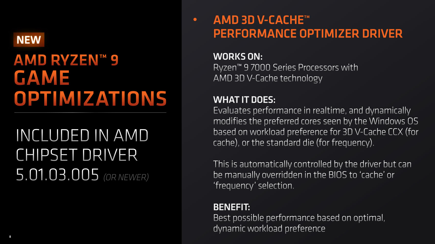
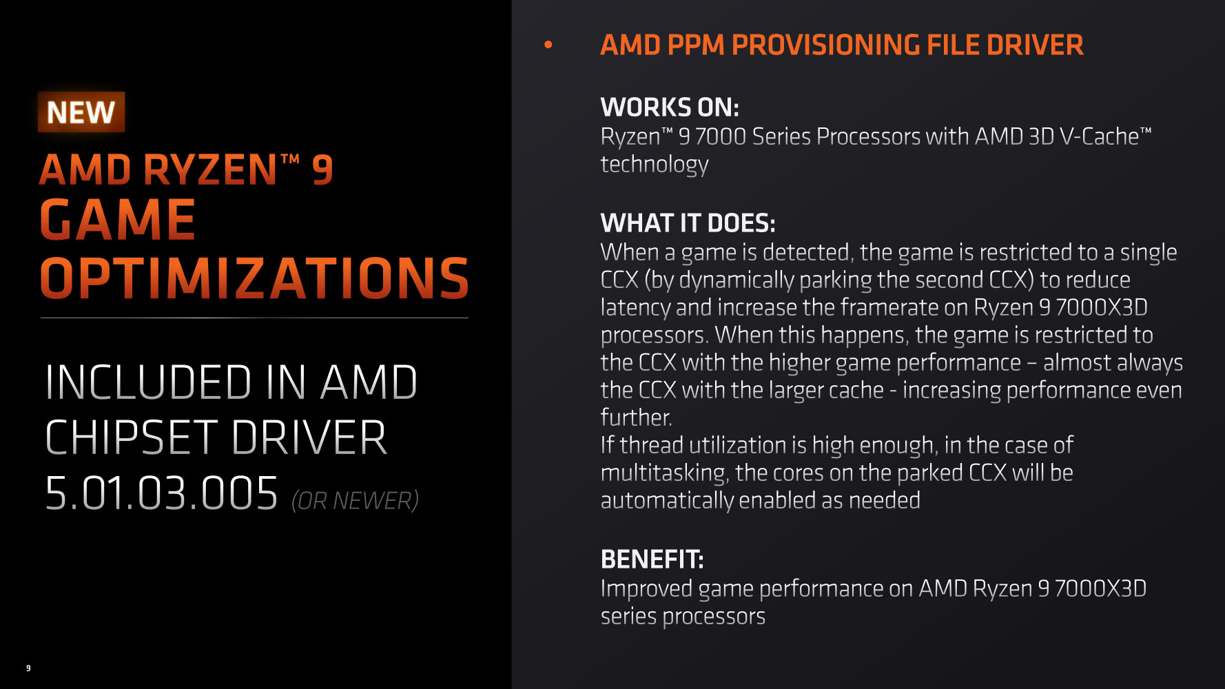
To make sure gaming workloads find the right CCD, AMD has implemented a high degree of software-level control, in the form of its 3D Vertical Cache Optimizer Driver, which is included with the latest version of AMD Chipset Software. This driver ensures that workload from games are directed to the CCD with the 3D Vertical Cache using dynamic "preferred cores" flagging for the Windows OS scheduler.
AMD Chipset Software includes a second relevant component, the PPM Provisioning File Driver. These drivers are typically involved in fine-grained collaborative power-management of the processor in response to performance demands from the OS, and play an especially important role on the mobile platform. For the 7950X3D, the latest PPM Provisioning File Driver does essentially the same action as the Cache Optimizer Driver, except using CPPC power-management controls. While the X3D CCD is handling the gaming workload, the cores of the second CCD are parked, and woken up as needed for background tasks.
Is this AMD's take on Hybrid Architecture? Not really, the CPU cores on both CCDs are the same "Zen 4" cores, with an identical ISA, it's just that there's some driver-level intelligence that makes sure 3D Vertical Cache benefits the applications that could use it. The second CCD without the stacked cache has the ability to boost to higher frequencies, and so the driver has the ability to direct specific kinds of workloads that benefit from a short burst of high-frequency, to that CCD.
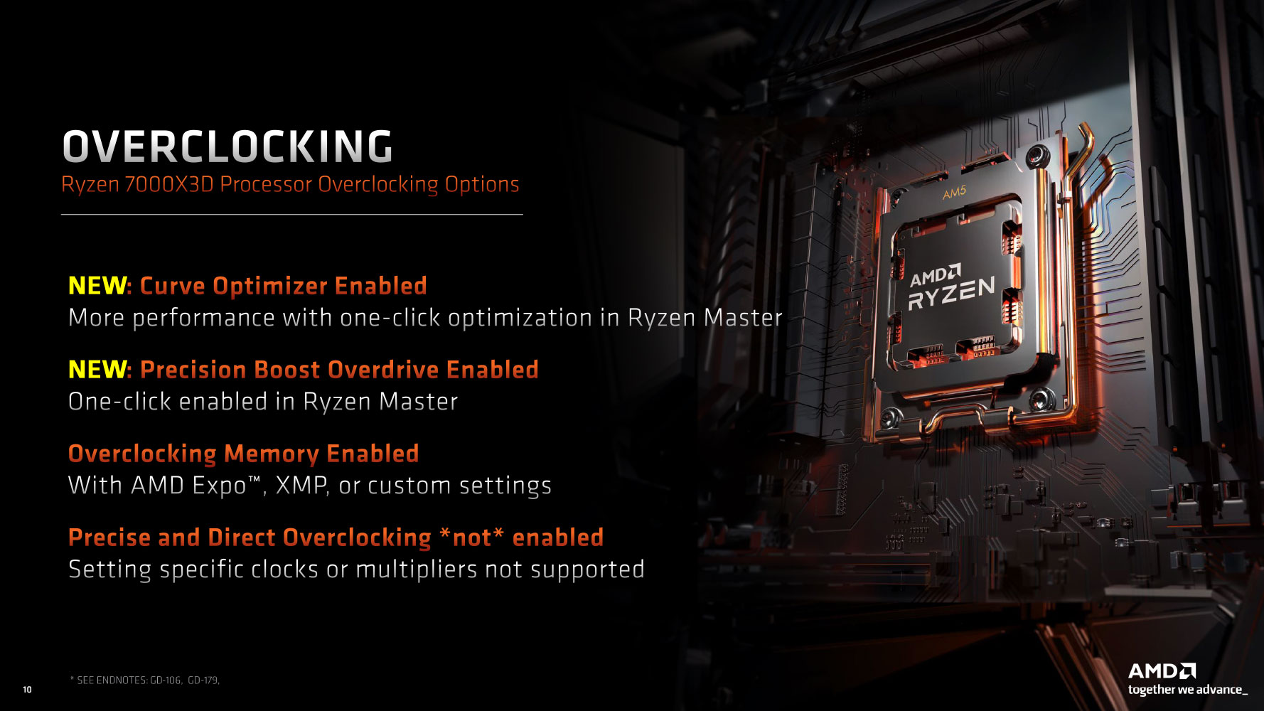
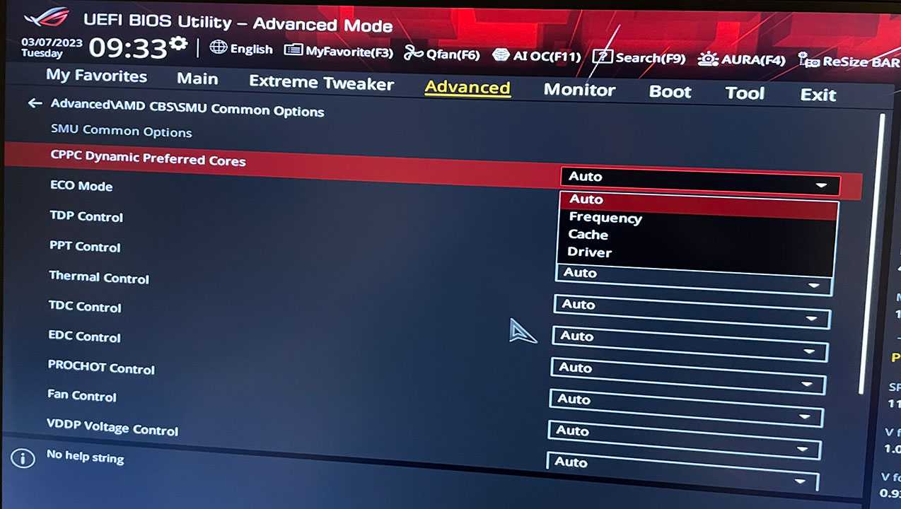
Unlike Intel Thread Director, the middleware responsible for making sure the right workload is handled by the ideal type of CPU cores on a Hybrid processor, AMD's Cache Optimizer driver gives you a degree of control via toggles in the motherboard's UEFI setup program (and possibly in the future through Ryzen Master). By default, you can leave the driver alone to do its thing, or you can take control, and tell it to "prefer cache," where all workload is prioritized to the CCD with the 3D Vertical Cache. The third toggle, "prefer frequency," prioritizes workloads to the second CCD without 3D Vertical Cache, which can sustain higher boost frequencies. Or you can just disable all optimization—this is only useful if you're poking around with the tech, or troubleshooting things. In our review, we've presented data for these modes. Also, unlike the previous-generation 5800X3D that lacked any notable overclocking capabilities, AMD is introducing a greater degree of overclocking with its 7000X3D series through Precision Boost Overdrive.
The Zen 4 Platform

AMD Zen has been one of the most remarkable turnarounds for a company in the semiconductor industry, and has had a profound impact on the consumer, as it influenced Intel's CPU core-counts. With each new generation of Zen, AMD delivered IPC and overall performance improvements, and Zen 4 stands out as it not only aims to improve performance, but also introduce a brand-new platform after five years of Socket AM4. As a parting gift, AMD enabled official Zen 3 support on even the oldest 300-series chipset, going to show just how consumer-friendly AM4 was, something the company hopes to repeat with AM5. The new AM5 socket was needed as the company enables the latest I/O, including DDR5 memory and PCI-Express Gen 5, besides power-delivery improvements. The socket can now deliver up to 230 W of power, which gives AMD room to increase CPU core-counts in the future. AM5 is a land-grid array, just like Intel desktop sockets, but the company retained CPU cooler compatibility with AM4.
Zen 4 Chip Configuration


The Ryzen 7000 series desktop processor, codenamed "Raphael," is a multi-chip module, just like the Ryzen 5000 "Vermeer" and Ryzen 3000 "Matisse." The CPU cores are located in specialized dies called CCDs (CPU complex dies), while the platform I/O control is located in a separate die called cIOD (client I/O die). The CCDs were fabricated on the latest TSMC 5 nm EUV (N5) node, while the cIOD are done so on TSMC 6 nm (N6) nodes. The idea here is that the parts that benefit the most from the switch to the latest foundry process—the CPU cores—are built on this node; while everything else that can do with a slightly older node, uses that instead. This way AMD can make the most of its 5 nm foundry allocation with TSMC. The MCM contains a cIOD, and two 8-core CCDs in case of the Ryzen 9 7950X and 7900X; or one 8-core CCD in case of the Ryzen 7 7700X and Ryzen 5 7600X. Infinity Fabric interconnect handles communications not just within these dies, but also between them. The transition to fast DDR5 memory and PCIe Gen 5 means that AMD now can push instructions and data around faster. It did so with microarchitectural improvements to the "Zen 4" core itself, while also increasing the Infinity Fabric bandwidth between the cores.
The Zen 4 CPU Core


All cores in Ryzen 7000 series processors are of the same kind, what Intel would consider a performance-core, or P-core. AMD has worked on all three key stages of the CPU—the front-end, the execution, and the load/store. The front-end is the "mouth" of the CPU core, and prepares data and instructions for execution. Front-end improvements begin at the Branch Prediction unit, which can how predict 2 taken branches per clock-cycle, and comes with larger L1 and L2 branch-target buffers (BTBs). AMD had for the very first time introduced an OpCache with Zen, improving it over time. AMD has increased the size of the OpCache by around 68 percent. It can now handle 9 macro-ops per cycle. The micro-op queue dispatch rate to the execution stage is still 6.

The Execution Stage is the main number-crunching machinery, and broadly features two components for the kind of math workload being executed—Integer and Floating Point. The "Zen 4" execution stage features a 25% larger instruction retire queue, larger register files, and higher buffer queue-depths throughout the core.


With "Zen 4," AMD is introducing support for AVX-512, in a bid to increase the processor's AI inferencing performance. The company did this in a die-area efficient, and energy-efficient manner, with no impact on CPU core frequency. AVX-512 operations are executed on a dual-pumped 256-bit FPU, rather than building ground-up 512-bit FP machinery. VNNI and Bfloat16 instruction-sets are also added, which mean that "Zen 4" can handle pretty much all of the AVX-512 client-relevant workloads that competing Intel processors can.

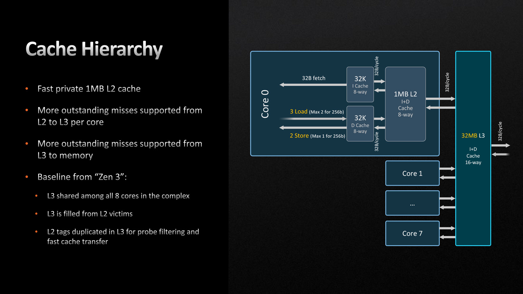
The Load/Store unit is the part of the core that interfaces with the memory sub-system. The "Zen 4" core gets a 22 percent larger Load Queue, with improved data-port conflict-resolution. There's a 50% larger L2 data transition lookaside buffer. The cache-hierarchy of the Ryzen 7000 desktop processor is similar to that of Ryzen 5000, with a few key differences, besides bandwidth/latency improvements—the dedicated L2 cache has been doubled in size to 1 MB per core. The eight CPU cores on a CCD share a monolithic 32 MB L3 cache, with uniform access to each core.

These improvements contribute to a 13 percent IPC improvement over "Zen 3," AMD claims. The company provided a break-up of which components are contributing to the IPC uplift, and we see that close to two-thirds of it are coming from improvements to the front-end and load/store stages. Branch prediction improvements contribute a fifth of this uplift. Interestingly, the L2 cache contributes barely 1/10th of the IPC uplift, in the tested applications—we believe this increase is mostly relevant for server applications where it should be able to make a difference. Intel's "Golden Cove" P-core comes with 1.25 MB L2 cache, and "Raptor Cove" features 2 MB. Despite the doubling in L2 cache sizes, the resulting increase in cache latency is very well contained (from 12 cycles on the 512 KB L2 of "Zen 3," to just 14 cycles on "Zen 4").

VBS (virtualization-based security) is the standard on new Windows 11 installs and gets activated automatically, unless you specifically disable it. Windows 11 Security Center already flags VBS not being enabled as a warning, similar to Antivirus being disabled or outdated. AMD made several improvements to the Virtualization feature-set, to reduce its performance impact in a VBS-enabled client environment. This includes speculation control, dual AVIC to go with the physical dual-APIC, and TSC_AUX virtualization.
New 6 nm IO Die
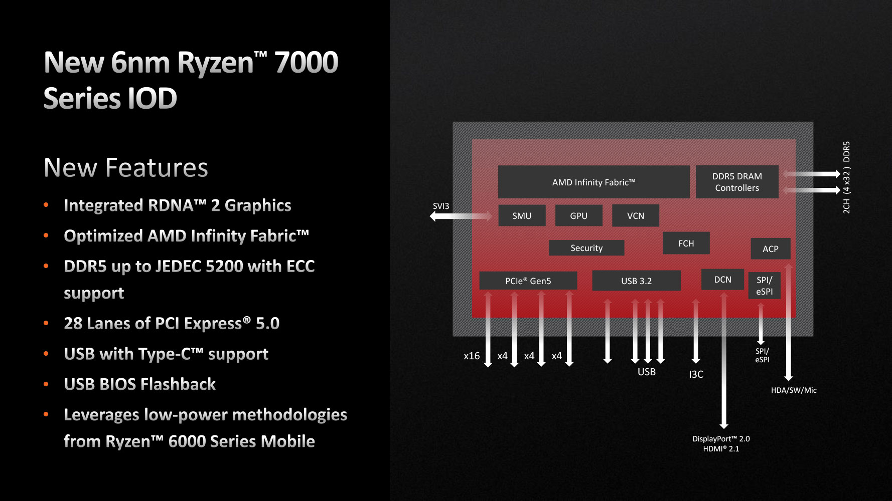
Ryzen 3000 "Matisse" and Ryzen 5000 "Vermeer" processors featured a cIOD built on the 12 nm FinFET Global Foundries node, but with Ryzen 7000 "Raphael," AMD is taking a giant leap toward improving the power characteristics of the cIOD, by building it on the new 6 nm TSMC node. This was needed mainly because the cIOD now packs an RDNA2 iGPU, besides the higher bandwidth switching fabric of the DDR5 and PCIe Gen 5 interfaces also warranting the change. The 12 nm previous-gen cIOD TDP was already estimated to be up to 15 W, and the addition of an iGPU would've thrown things off gear. In addition to 6 nm, AMD is deploying several of the power-management features of the Ryzen 6000-series "Rembrandt" mobile processor on this cIOD, which mainly have to do with aggressive power management and rapid sleep/wake for the various components on the die.
The new 6 nm cIOD packs a dual-channel DDR5 memory controller (4x 40-bit channels, including ECC and hardware-accelerated encryption support), with native support for DDR5-5200; a PCI-Express 5.0 x28 root-complex; a USB 3.2 controller with support for 20 Gbps 2x2 ports, USB-C, and DisplayPort passthrough from the iGPU. AMD was very clear that the inclusion of an iGPU doesn't make "Raphael" an APU, because the iGPU is rather basic, just about enough for non-gaming workloads. The company intends to continue making APUs—processors with beefy iGPUs for mainstream gaming performance—including for the desktop platform. Full ECC support on desktop is technically possible, but it will depend on the motherboard manufacturers—AMD isn't doing anything to prevent them from making their boards ECC compatible.
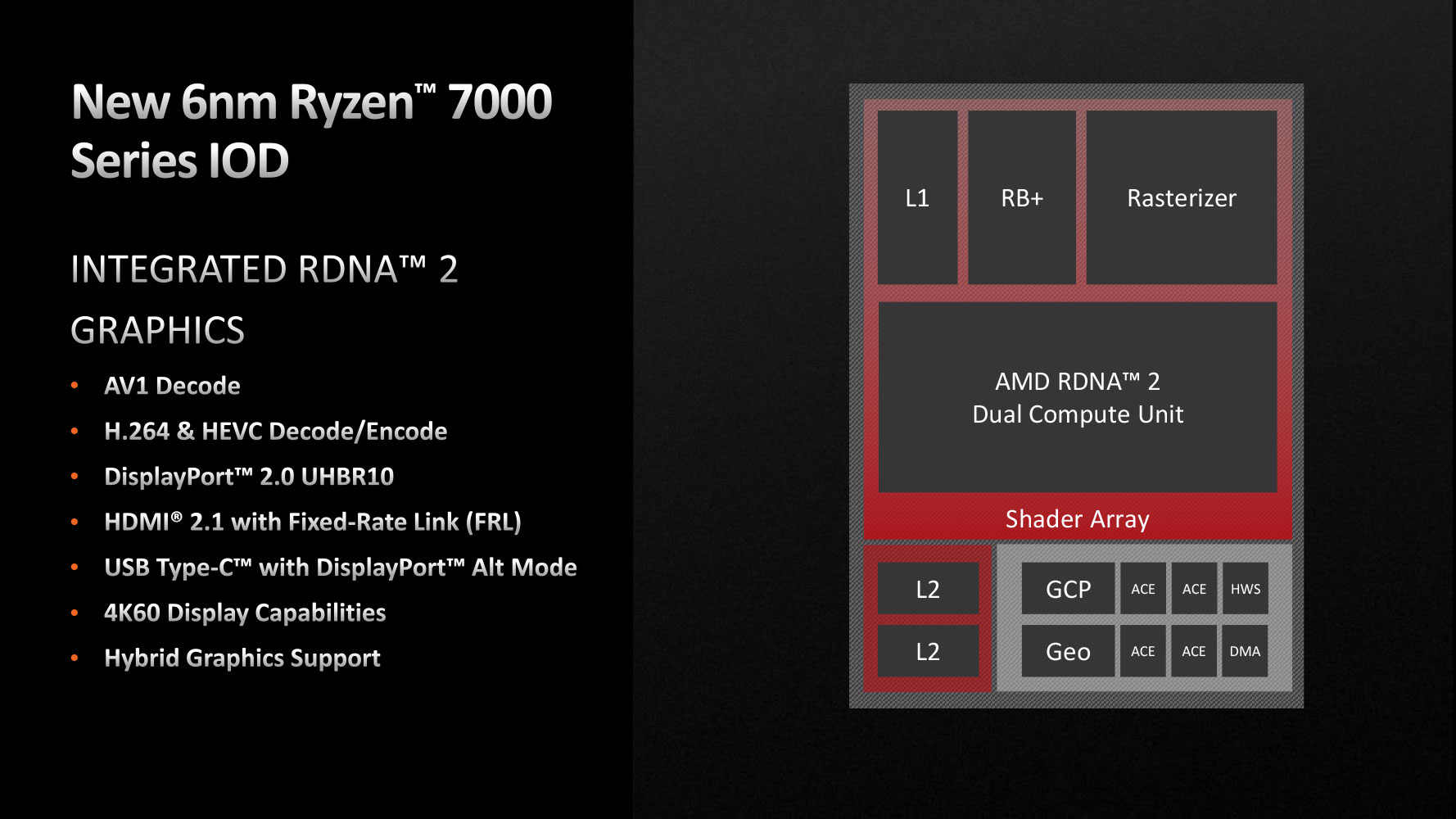
The Radeon 610 iGPU is based on the RDNA2 graphics architecture, and packs just two Compute Units, which work out to 128 stream processors. The Display CoreNext (DCN) and Video CoreNext (VCN) components are of modern design. The VCN offers hardware-accelerated AV1 and H.265 decode, as well as hardware-accelerated H.265 encode. Just to clarify, there is hardware AV1 decode support, but no encode, which isn't a big deal at all. In terms of monitors, the DCN supports DisplayPort 2.0 UHBR10, HDMI 2.1 with FRL, and DisplayPort passthrough for the USB type-C ports connected to the on-die USB 3.2 controller. When paired with a discrete graphics card on Windows 10 or Windows 11, the iGPU supports Hybrid graphics, much in the same way as it's implemented on notebooks. You plug in your monitor to the iGPU, and it wakes up your discrete GPU (graphics card) when needed. The RDNA2 compute units are of the same kind you'd find in Radeon RX 6000 series GPUs, including ray tracing support, but this is of no use on the Radeon 610. The only reason AMD went with RDNA2 is because it can offer comparable levels of performance with just two CUs, to a "Vega" based iGPU that would need more CUs (thereby increasing die-size).
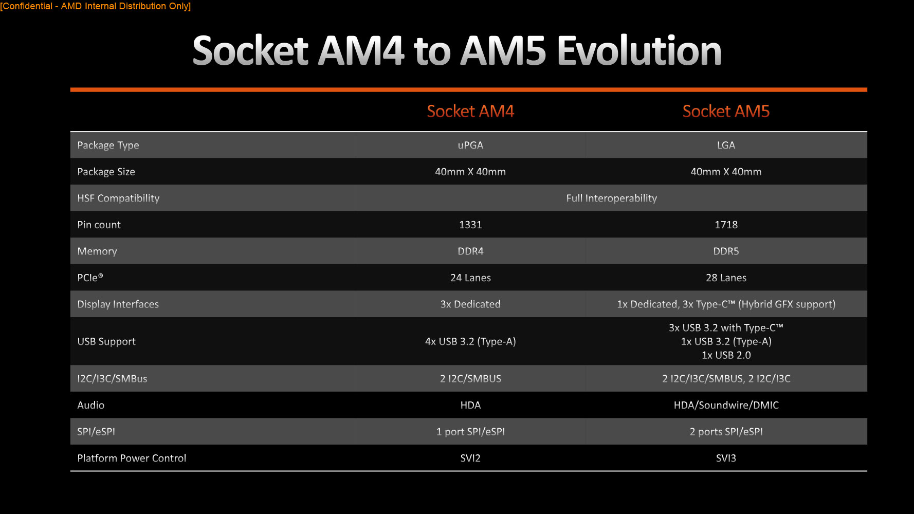
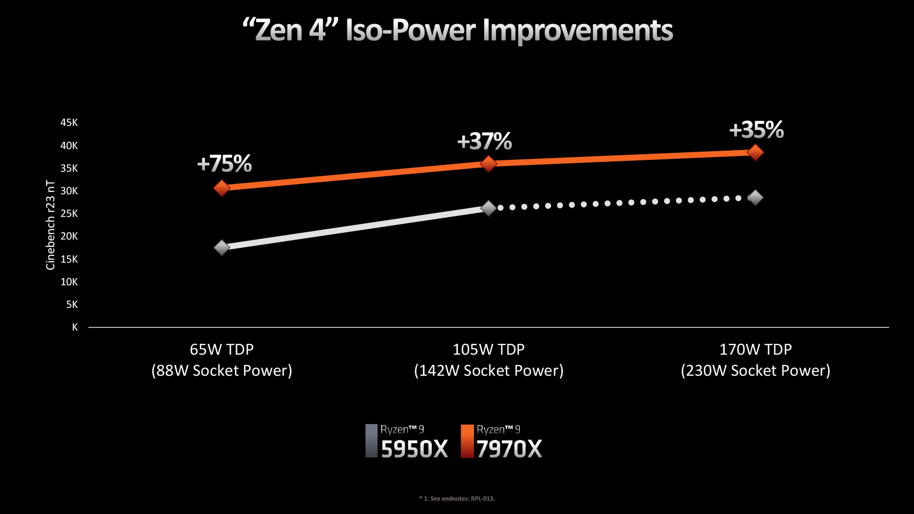
As we mentioned earlier, AMD needed a new socket as it was transitioning to DDR5 and PCIe Gen 5, which come with stiff physical-layer signaling requirements that AM4 couldn't provide. AM5 also makes processors "future-ready" as it enables two-way communication with the voltage regulators. The added pin-count was needed not just for DDR5 and its 40-bit sub-channels, but also for four additional PCIe lanes. The processor puts out a total of 28 PCIe Gen 5 lanes. 16 of these are meant for PEG (graphics card slots); 4 serve as chipset bus, and 8 lanes are available for the motherboard vendors to play around with: either wiring them both out as M.2 Gen 5 x4 slots, or wire one of them as M.2, and use the remaining 4 lanes for high-bandwidth devices, such as discrete USB4 controllers, 80 Gbps Thunderbolt 4 controllers, or even CPU-attached low-latency network interfaces. AM5 also significantly increases power-delivery capability over AM4—up to 230 W. The increased power should enable the "Zen 4" cores to run at very high clock-speeds approaching the 6 GHz-mark, or in the future, even enable core-count increases.

The clock-domains of Ryzen 7000 are similar to those of the Ryzen 5000 series. FCLK defines the Infinity Fabric clock-speed, which is de-linked from UCLK (memory controller clock), and MCLK (DRAM clock). AMD says that DDR5-6000 strikes the "sweetspot" in that this is the highest MCLK you can run while retaining certain memory overclocker optimizations. On Zen 3 you'd want to run Infinity Fabric in sync with memory, but this isn't possible anymore, because FCLK can't reach 3000 MHz (assuming DDR5-6000 memory). Now the optimum config is to run FCLK at 2000, basically a 3:2 divider. Picking "auto" in the BIOS will automatically aim for that setting. Above 6000 MHz, the strategy will be changed to 2:1 ratio.
AMD X670E and B650E Chipsets
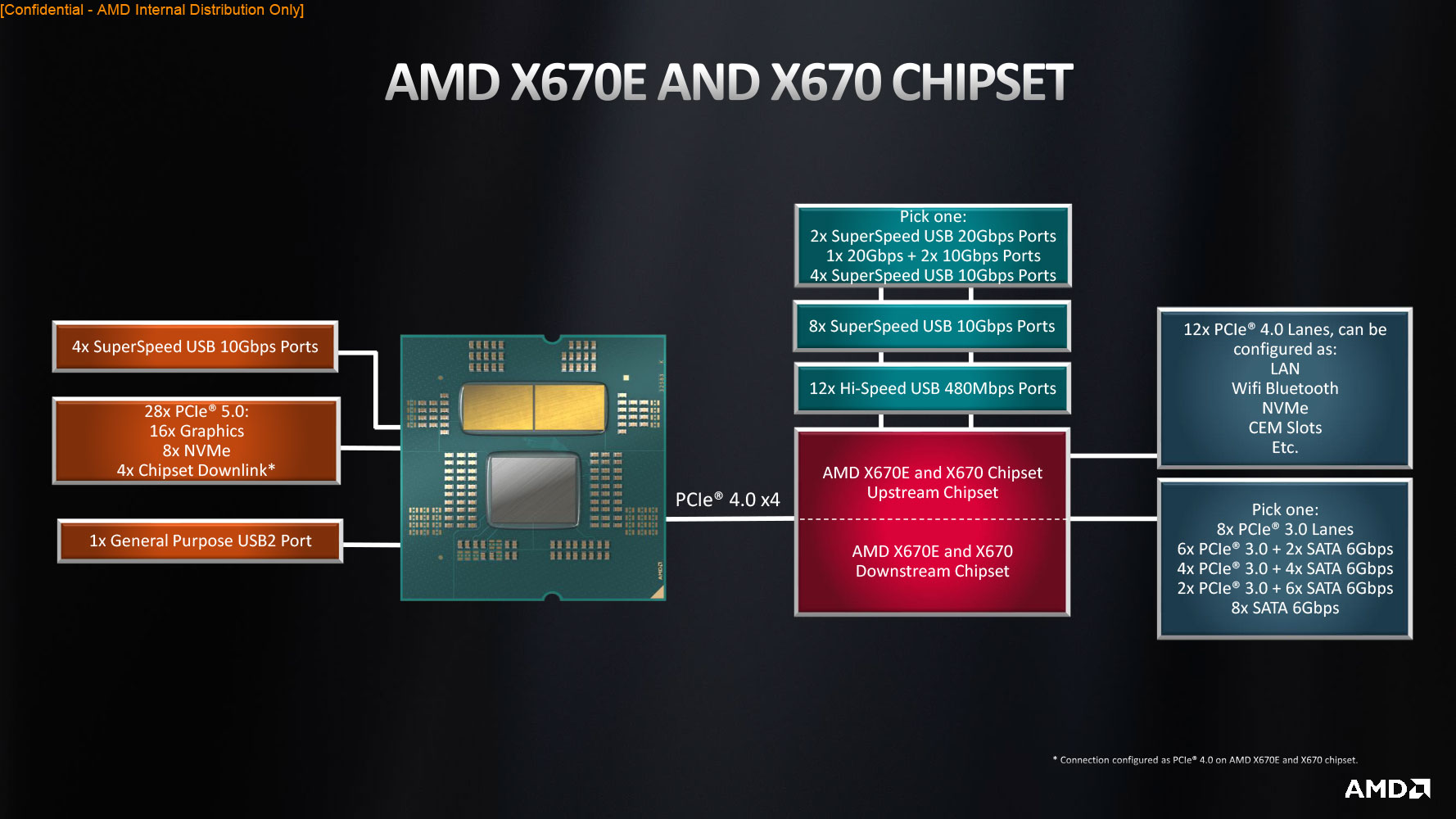
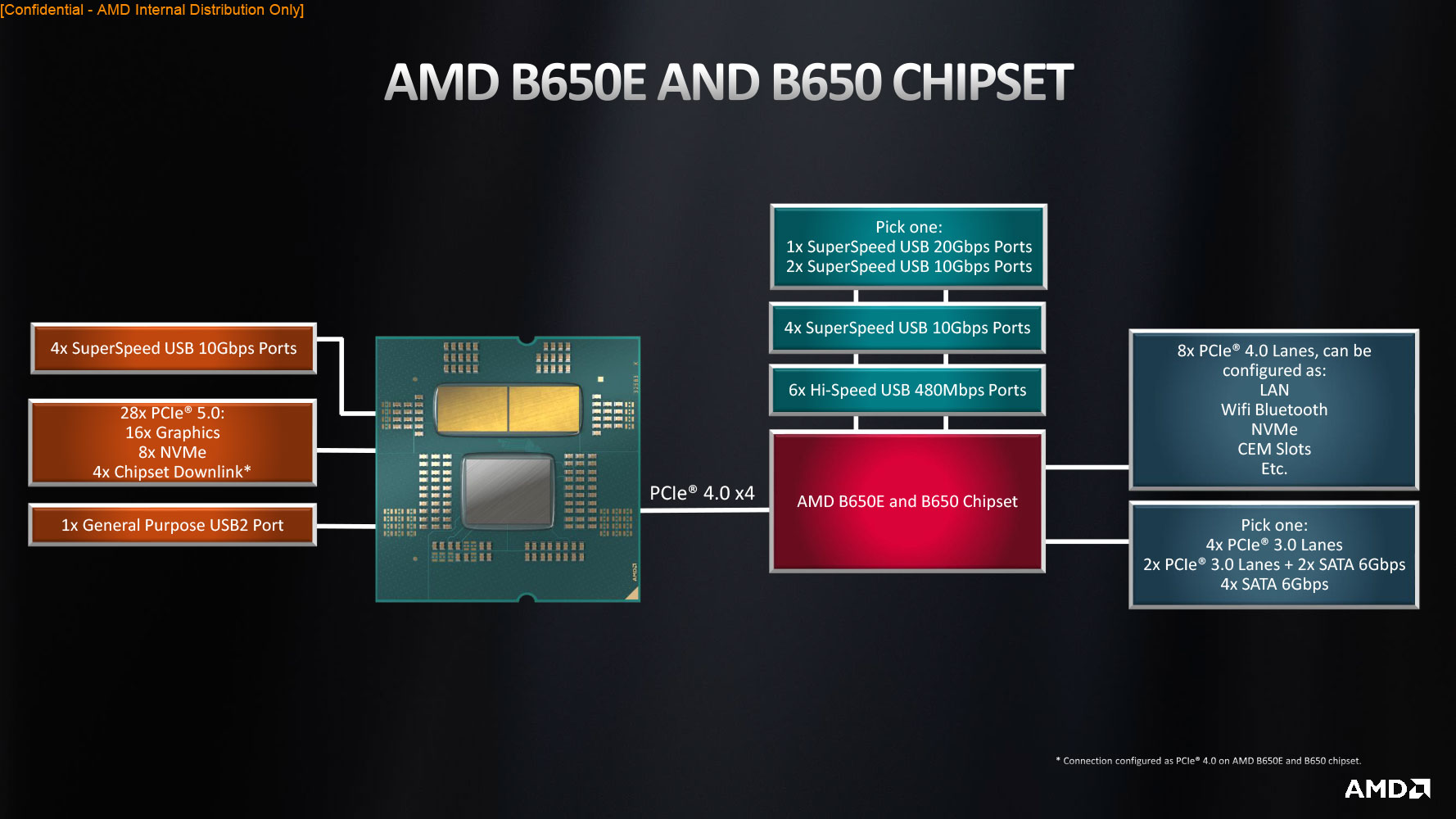
AMD took a unique approach to chipsets with this generation. The top-tier chipset now comes in two flavors, X670E and X670. Both are identical in downstream I/O, but the X670E offers PCIe Gen 5 PEG besides CPU-attached Gen 5 NVMe; whereas the X670 only offers Gen 5 on the CPU-attached M.2 NVMe slot, but not PEG (which is Gen 4). A similar approach is taken when segregating the mid-tier B650E from the B650. The lack of Gen 5 PEG should significantly reduce motherboard costs, as designers would be saving on both Gen 5 redrivers and the steep wiring requirements to avoid signal-corruption.
X670E is a 2-chip chipset unlike the previous-gen X570. This was done to increase the downstream PCIe connectivity. The chipset now offers up to 12x PCIe Gen 4 and up to 8x PCIe Gen 3 downstream lanes (not counting the lanes from the CPU). This lets motherboard designers wire out three additional M.2 Gen 4 slots attached to the chipset, while the Gen 3 lanes handle low-bandwidth onboard devices. AMD adopted a wacky way to connect the two bridges that make up the chipset. There is an "upstream" chipset that's wired to the AM5 SoC over a PCI-Express 4.0 x4 connection; the second bridge is called "downstream" chipset, and is connected to four of the PCIe Gen 4 downstream lanes of the "upstream" chipset. The X670/E puts out up to two 20 Gbps USB 3.2, up to eight 10 Gbps USB 3.2, and twelve USB 2.0. The B650E and B650 look like more reasonable single-chip chipsets. They talk to the SoC over PCI-Express 4.0 x4, and wire out 8x PCIe Gen 4 downstream lanes, and up to 4x PCIe Gen 3 downstream lanes. You get half the number of USB SuperSpeed ports as the X670/E.
AMD EXPO Memory
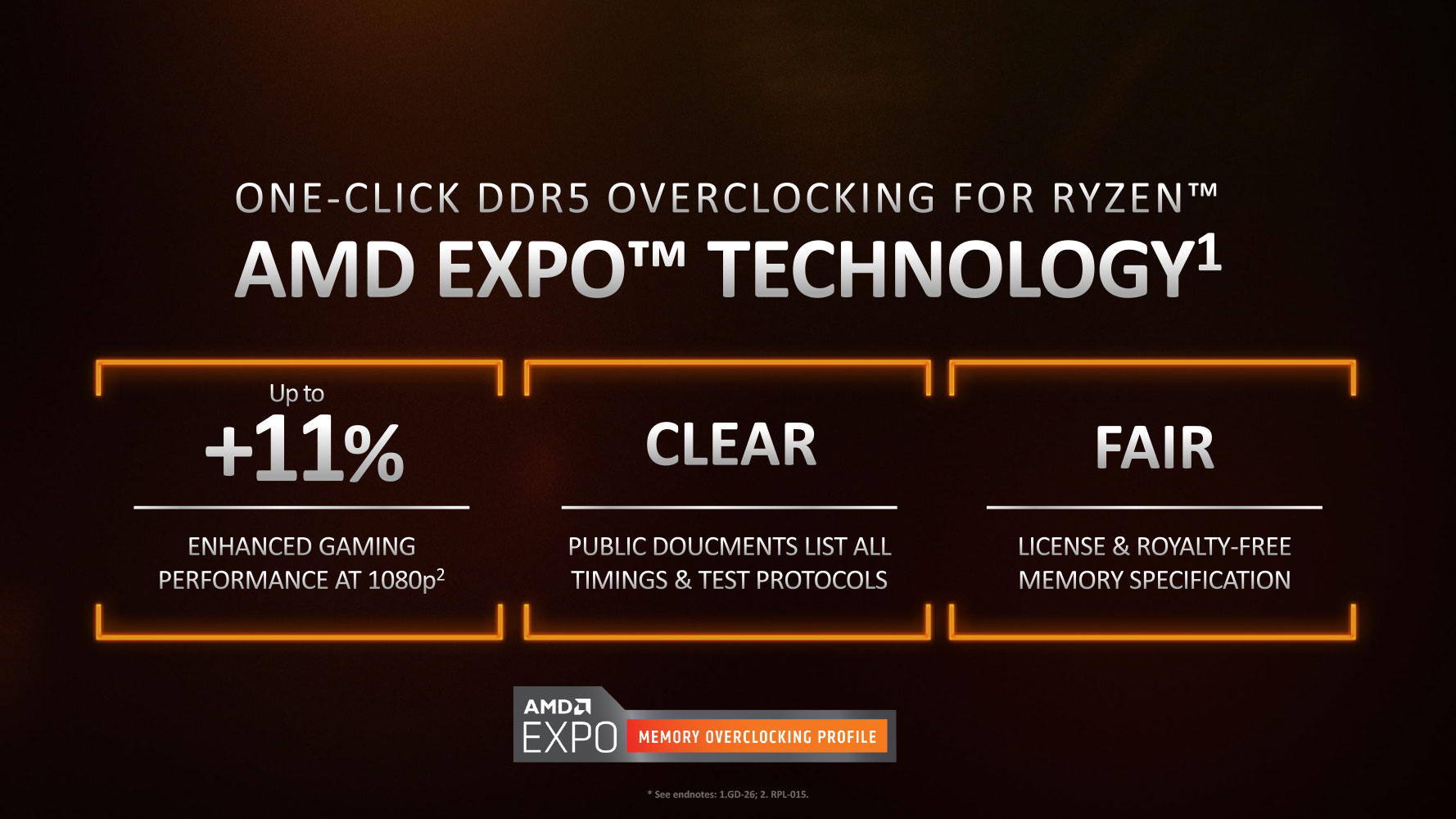

With Ryzen 7000 series, AMD is introducing EXPO (extended profiles for overclocking); a feature that's identical in concept to Intel XMP. AMD EXPO-certified DDR5 modules come with an easy method of applying the advertised memory speeds and timings—you simply select a toggle in the opening screen of your motherboard's UEFI BIOS program. EXPO differs from XMP in that it includes fine settings that are unique to the AMD architecture, and it's also an open standard. Until now, XMP modules installed on AMD systems relied either on painstaking manual overclocking, or use of DOCP, a feature that attempts to translate the settings in the XMP profile to "nearest neighbors" of AMD-compatible settings. This was sub-optimal. EXPO is royalty-free compared to XMP, so any memory manufacturer can implement it for free. Ryzen 7000 can run any PC-DDR5 memory in the market, including XMP-certified ones, so don't fret if you can't find EXPO kits just yet.
Our Patreon Silver Supporters can read articles in single-page format.
May 13th, 2024 05:22 EDT
change timezone
Latest GPU Drivers
New Forum Posts
- Purchased an AX1200i PSU as part of some forward planning, what tier is this PSU? (60)
- Long AM5 POST times (148)
- have LGA 1155 motherboard which xeon processor will fit ? (1)
- Soundbar or 2.1 speaker for virtual 3d audio in PC games... (13)
- AIO Water Cooler vs Tower Air Cooler (10)
- Flash VBIOS to turn RX 580 2048SP into RX 570 (39)
- PSU Option for my PC (12)
- Looking for a new case, cube shaped only. (5)
- LOL ASUS says this is $200 in repair, Steve from gamers Nexus smokes ASUS, Steam Deck til I die boys!!!! (77)
- Cyberpunk 2077 Game Discussion (2126)
Popular Reviews
- ZMF Caldera Closed Planar Magnetic Headphones Review
- Corsair MP700 Pro SE 4 TB Review
- Bykski CPU-XPR-C-I CPU Water Block Review - Amazing Value!
- ThundeRobot ML903 NearLink Review
- Upcoming Hardware Launches 2023 (Updated Feb 2024)
- CHERRY XTRFY M64 Pro Review
- AMD Ryzen 7 7800X3D Review - The Best Gaming CPU
- ASUS Radeon RX 7900 GRE TUF OC Review
- Corsair iCUE Link RX120 RGB 120 mm Fan Review
- Sapphire Radeon RX 7900 GRE Pulse Review
Controversial News Posts
- Intel Statement on Stability Issues: "Motherboard Makers to Blame" (266)
- AMD to Redesign Ray Tracing Hardware on RDNA 4 (224)
- Windows 11 Now Officially Adware as Microsoft Embeds Ads in the Start Menu (171)
- NVIDIA to Only Launch the Flagship GeForce RTX 5090 in 2024, Rest of the Series in 2025 (151)
- Sony PlayStation 5 Pro Specifications Confirmed, Console Arrives Before Holidays (119)
- AMD's RDNA 4 GPUs Could Stick with 18 Gbps GDDR6 Memory (114)
- AMD Hits Highest-Ever x86 CPU Market Share in Q1 2024 Across Desktop and Server (110)
- AMD Ryzen 9 7900X3D Now at a Mouth-watering $329 (104)