 62
62
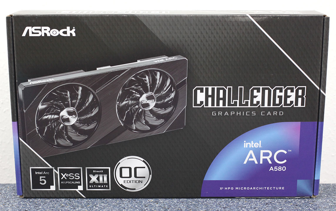
ASRock Arc A580 Challenger Review
(62 Comments) »Introduction
ASRock Arc A580 Challenger is the company's custom-design graphics card that debuts Intel's latest and most interesting addition to the desktop GPU space. The new A580 Alchemist comes in at a disruptive starting price of just $180, offering 1080p gaming with high through enthusiast settings, the full DirectX 12 Ultimate feature-set, including real time ray tracing, and XeSS performance enhancement. For these reasons, and the fact that it's based on the contemporary 6 nm foundry node, the A580 is every bit a current-generation GPU, designed to appeal to the class of people entering the PC gaming segment, and could do with a trusty brand like Intel.

Why Intel decided to launch the A580 now, nearly a year after its Arc 7-series debut, can be explained with two distinct theories: first, prices of graphics cards are finally cooling down, which brought 1080p-class graphics cards down to around $250, presenting Intel with an opportunity to undercut products such as the GeForce RTX 3050 and Radeon RX 6600 at $180; Intel has taken huge strides over the past year towards upgrading the software backbone of its Arc GPUs, which effectively push each product a segment above. This has been done with dozens of game-specific improvements, as well as API-specific uplifts for DirectX 11 and DirectX 9, which are still relevant for popular e-sports titles.
The Arc A580 is based on the Xe-HPG Alchemist graphics architecture, which is a thorough, grounds-up attempt by Intel to engineer a contemporary discrete GPU that isn't missing out on any kind of feature compared to the latest GeForce RTX and Radeon RX GPUs. The GPUs also feature a real time ray tracing engine that's technically more advanced than the one AMD uses, with hardware acceleration for even more stages of the ray tracing, full asynchrony with ray tracing, and shader re-ordering. The GPU also features XMX a dedicated matrix math accelerator that makes these GPUs AI processing powerhouses, something Intel leverages for its XeSS performance enhancement that's technologically at par with DLSS 2.
Intel carved the Arc A580 out of the same 6 nm ACM-G10 silicon powering the company's Arc 7 series. The new SKU is endowed with 24 out of the 32 Xe Cores physically present on the silicon, across 6 out of 8 Render Slices. This works out to 384 execution units, which are worth 3,072 unified shaders, 384 XMX cores, 24 Ray Tracing Engines, 192 TMUs, and 96 ROPs.
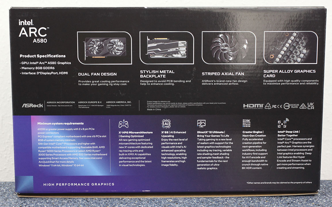
The most interesting aspect of the A580 is that it gets the same exact memory sub-system as the A750. There's 8 GB of GDDR6 memory on offer, across a wide 256-bit memory bus, which paired with its 16 Gbps memory speed, yields 512 GB/s of memory bandwidth, the highest in the market segment. That's not all, the A580 has the full PCI-Express 4.0 x16 host interface, compared to its rivals, which usually come with truncated Gen 4 x8 interfaces. What this means is that you get uncompromised performance on older PCIe Gen 3 platforms such as the 10th Gen Core "Comet Lake" or Ryzen 2000, which support Resizable BAR (something that's required for Arc GPUs to reach their advertised performance).
We've known the Challenger line of graphics cards from ASRock with a several lines of AMD Radeon graphics cards. These cards represent the company's value custom-designs, with compact product designs, a cooler focused on low-noise and easy serviceability; and a price that's usually close to the GPU's baseline, which in this case, is $180. The ASRock Arc A580 Challenger is for those that just want an A580 that they can install and forget about.
Short 5-Minute Video Overview
Our goal with these videos is to create short summaries, not go into all the details and test results, which can be found in our written reviews.
| Price | Cores | ROPs | Core Clock | Boost Clock | Memory Clock | GPU | Transistors | Memory | |
|---|---|---|---|---|---|---|---|---|---|
| RX 5500 XT | $170 | 1408 | 32 | 1717 MHz | 1845 MHz | 1750 MHz | Navi 14 | 6400M | 4 GB, GDDR6, 128-bit |
| RX 5600 XT | $190 | 2304 | 64 | 1375 MHz | 1560 MHz | 1500 MHz | Navi 10 | 10300M | 6 GB, GDDR6, 192-bit |
| RX 6500 XT | $150 | 1024 | 32 | 2685 MHz | 2825 MHz | 2248 MHz | Navi 24 | 5400M | 4 GB, GDDR6, 64-bit |
| RTX 2060 | $160 | 1920 | 48 | 1365 MHz | 1680 MHz | 1750 MHz | TU106 | 10800M | 6 GB, GDDR6, 192-bit |
| Arc 580 | $180 | 3072 | 96 | 1700 MHz | N/A | 2000 MHz | ACM-G10 | 21700M | 8 GB, GDDR6, 256-bit |
| ASRock Arc 580 Challenger | $180 | 3072 | 96 | 1700 MHz | N/A | 2000 MHz | ACM-G10 | 21700M | 8 GB, GDDR6, 256-bit |
| RX 5700 XT | $150 | 2560 | 64 | 1605 MHz | 1755 MHz | 1750 MHz | Navi 10 | 10300M | 8 GB, GDDR6, 256-bit |
| RTX 3050 | $210 | 2560 | 32 | 1552 MHz | 1777 MHz | 1750 MHz | GA106 | 12000M | 8 GB, GDDR6, 128-bit |
| RTX 2070 | $200 | 2304 | 64 | 1410 MHz | 1620 MHz | 1750 MHz | TU106 | 10800M | 8 GB, GDDR6, 256-bit |
| Arc A750 | $190 | 3584 | 112 | 2050 MHz | N/A | 2000 MHz | ACM-G10 | 21700M | 8 GB, GDDR6, 256-bit |
| RX 6600 | $170 | 1792 | 64 | 2044 MHz | 2491 MHz | 1750 MHz | Navi 23 | 11060M | 8 GB, GDDR6, 128-bit |
| RX 6600 XT | $200 | 2048 | 64 | 2359 MHz | 2589 MHz | 2000 MHz | Navi 23 | 11060M | 8 GB, GDDR6, 128-bit |
| RTX 3060 | $240 | 3584 | 48 | 1320 MHz | 1777 MHz | 1875 MHz | GA106 | 12000M | 12 GB, GDDR6, 192-bit |
| RX 7600 | $240 | 2048 | 64 | 2250 MHz | 2625 MHz | 2250 MHz | Navi 33 | 13300M | 8 GB, GDDR6, 128-bit |
| RTX 4060 | $280 | 3072 | 48 | 1830 MHz | 2460 MHz | 2125 MHz | AD107 | 18900M | 8 GB, GDDR6, 128-bit |
| Arc A770 | $290 | 4096 | 128 | 2100 MHz | N/A | 2187 MHz | ACM-G10 | 21700M | 16 GB, GDDR6, 256-bit |
| RTX 2080 | $240 | 2944 | 64 | 1515 MHz | 1710 MHz | 1750 MHz | TU104 | 13600M | 8 GB, GDDR6, 256-bit |
| RTX 3060 Ti | $260 | 4864 | 80 | 1410 MHz | 1665 MHz | 1750 MHz | GA104 | 17400M | 8 GB, GDDR6, 256-bit |
| RTX 4060 Ti | $370 | 4352 | 48 | 2310 MHz | 2535 MHz | 2250 MHz | AD106 | 22900M | 8 GB, GDDR6, 128-bit |
| RX 6700 XT | $310 | 2560 | 64 | 2424 MHz | 2581 MHz | 2000 MHz | Navi 22 | 17200M | 12 GB, GDDR6, 192-bit |
| RTX 2080 Ti | $350 | 4352 | 88 | 1350 MHz | 1545 MHz | 1750 MHz | TU102 | 18600M | 11 GB, GDDR6, 352-bit |
| RTX 3070 | $300 | 5888 | 96 | 1500 MHz | 1725 MHz | 1750 MHz | GA104 | 17400M | 8 GB, GDDR6, 256-bit |
| RTX 3070 Ti | $390 | 6144 | 96 | 1575 MHz | 1770 MHz | 1188 MHz | GA104 | 17400M | 8 GB, GDDR6X, 256-bit |
Architecture
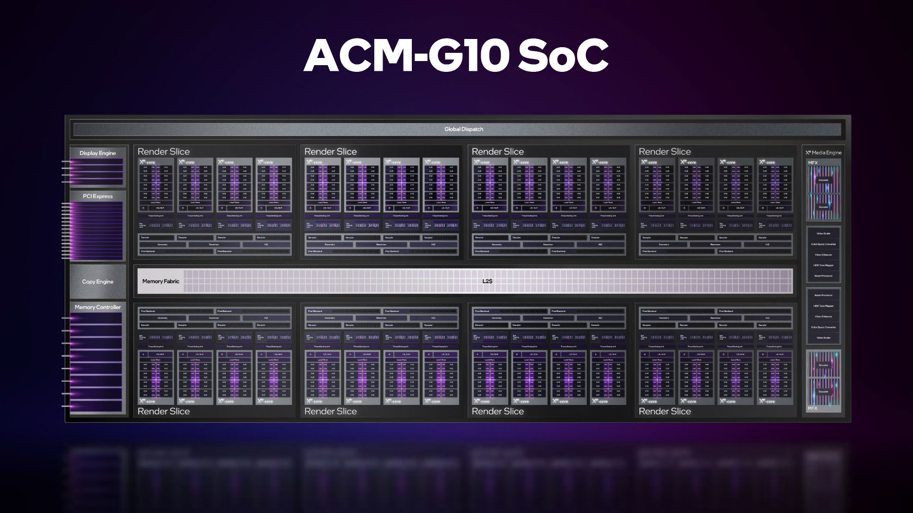
Intel Xe-HPG "Alchemist" graphics architecture sees its biggest implementation to date with the ACM-G10 silicon powering the A770, A750, and the new A580. Built on the 6 nm process at TSMC, the ACM-G10 measures 406 mm² in die-area, and packs 21.7 billion transistors. Much like NVIDIA and AMD, Intel has innovated its own hierarchy for the number-crunching machinery of its GPUs, and differentiates SKUs by changing the number of indivisible groups of these to meet performance targets. The ACM-G10 silicon features a PCI-Express 4.0 x16 host interface, a 256-bit wide GDDR6 memory interface, the Xe Media Engine and Xe Display Engine, among a global dispatch processor, and memory fabric that's cushioned by L2 cache. The main SIMD component top-level organization is the Render Slice. Each of these is a self-contained unit with all the number-crunching and raster graphics hardware a GPU needs.


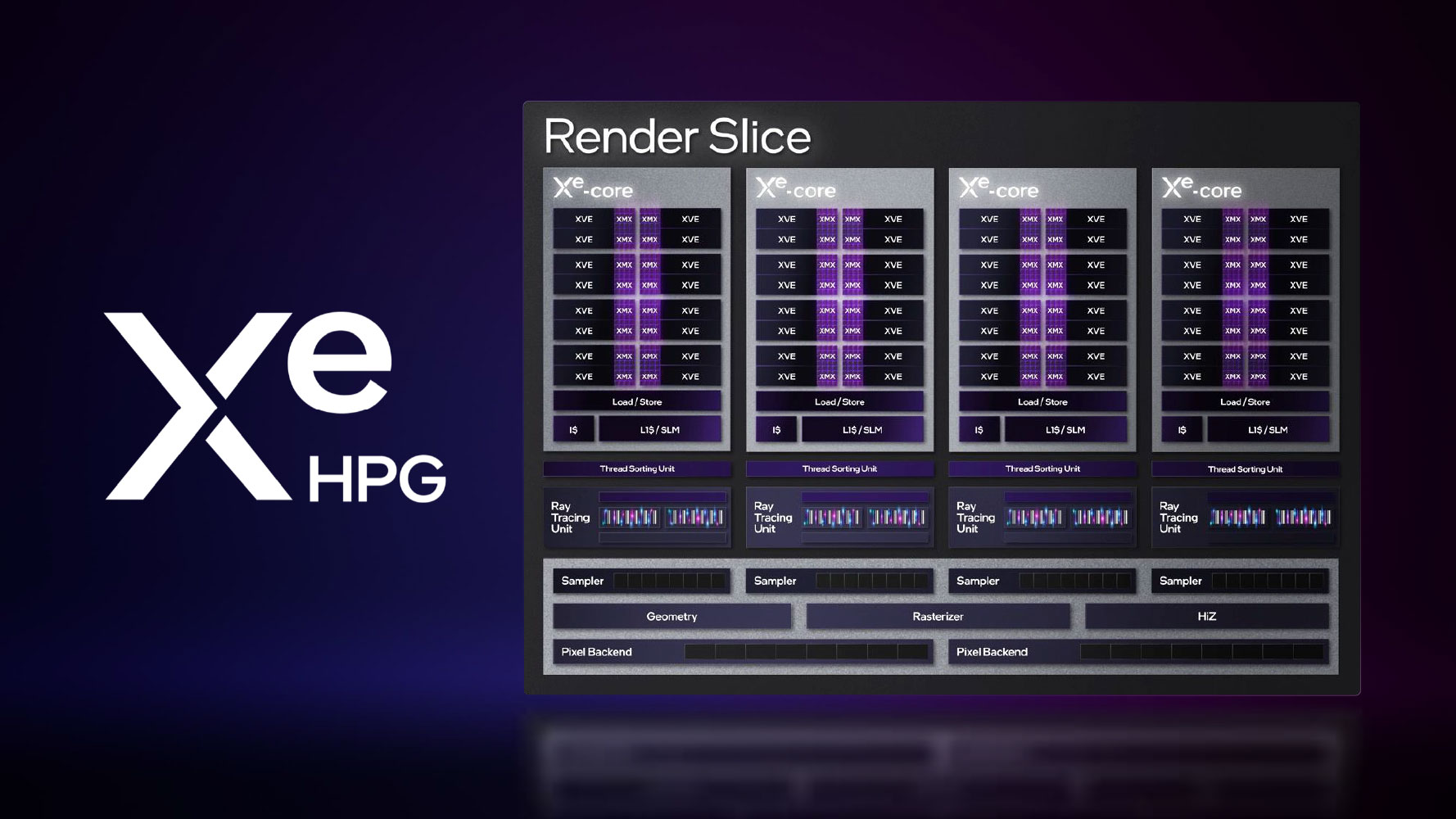
The ACM-G10 features eight such Render Slices. Each of these features four blocks of indivisible processing machinery, called Xe Cores; four Ray Tracing Units (RT units), and DirectX 12 Ultimate optimized raster-graphics units that includes four Samplers, Tessellation geometry processors, 16 ROPs, and 32 TMUs. Since there are 8 Render Slices, the silicon physically has 16 RT units, 128 ROPs, and 256 TMUs.
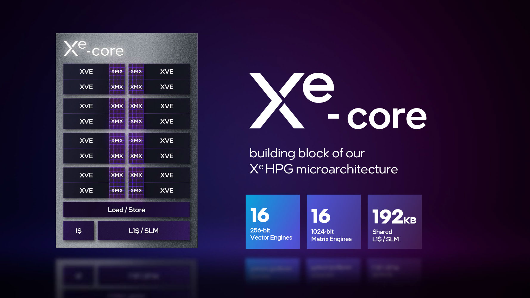

The Xe Core is the indivisible computation core, with sixteen 256-bit Vector Engines (execution units), sixteen 1024-bit XMX Matrix Engines, and 192 KB of L1 cache. Each Vector Engine has eight each of FP and INT units, besides a register file. Two adjacent Vector Engines share a Thread Control unit to share execution waves. There are 16 VEs per Xe Core, 4 Xe Cores per Render Slice, and 8 Render Slices on the ACM-G10 silicon, so we have 512 execution units in all, each with 8 FP/INT execution stages, which logically work out to 4,096 unified shaders. The A580 is carved out of this silicon by leaving the memory sub-system untouched, but enabling just 24 out of 32 Xe cores, by disabling two Render Slices. This results in 384 execution units, or 3,072 unified shaders, 384 XMX cores for AI acceleration, 24 Ray Tracing Engines, 192 TMUs, and 96 ROPs.
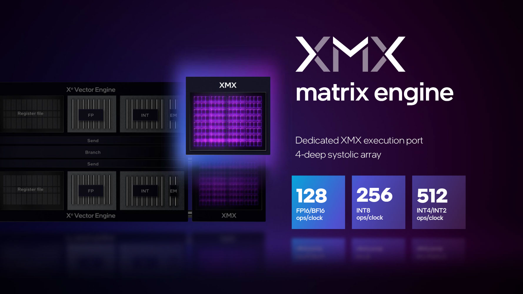
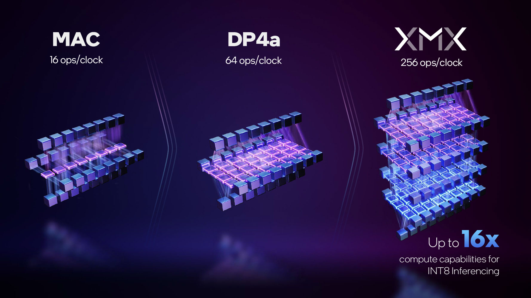
The XMX Matrix Engine is an extremely capable matrix-multiplication fixed-function hardware that can accelerate AI deep-learning neural net building and training. It's also a highly capable math accelerator. Intel originally designed this technology for the Xe-HP AI processors, but it finds client applications in Arc Graphics, where it is leveraged for ray tracing denoising and to accelerate features such as XeSS. There are 16 XMX units per Xe Core, and 64 per Render Slice, 512 across the ACM-G10 silicon. Each XMX unit can handle 128 FP16 or BF16 operations per clock; up to 256 INT8 ops/clock, and 512 INT4 ops/clock. The XMX-optimized native XeSS code is an order of magnitude faster than the industry-standard DP4a codepath of XeSS, as you'll see in our testing.
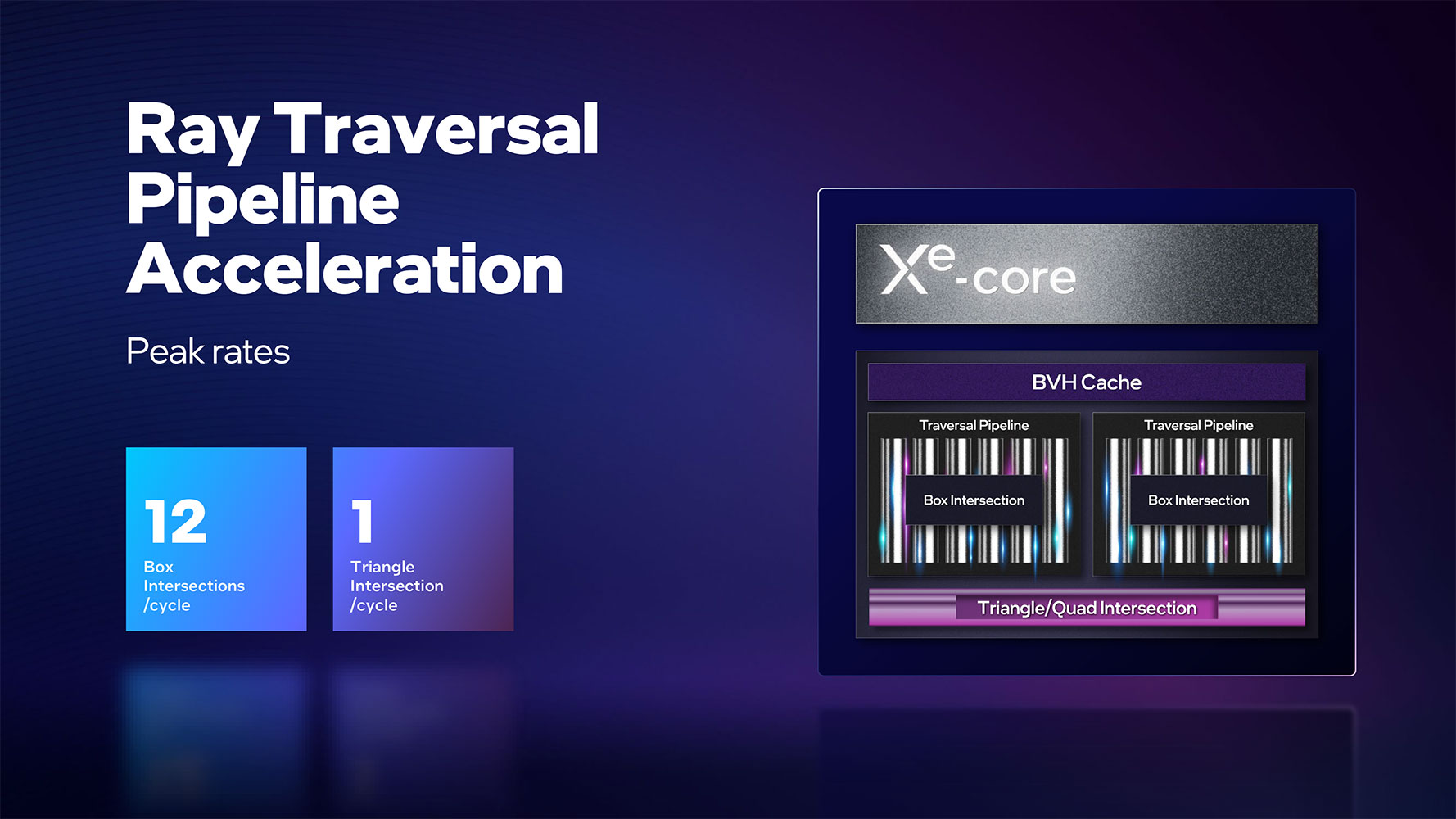

When it comes to real time ray tracing, Intel's Xe-HPG architecture has technological-parity with NVIDIA RTX, due to its heavy reliance on fixed-function hardware for ray intersection, BVH, and AI-based denoising.
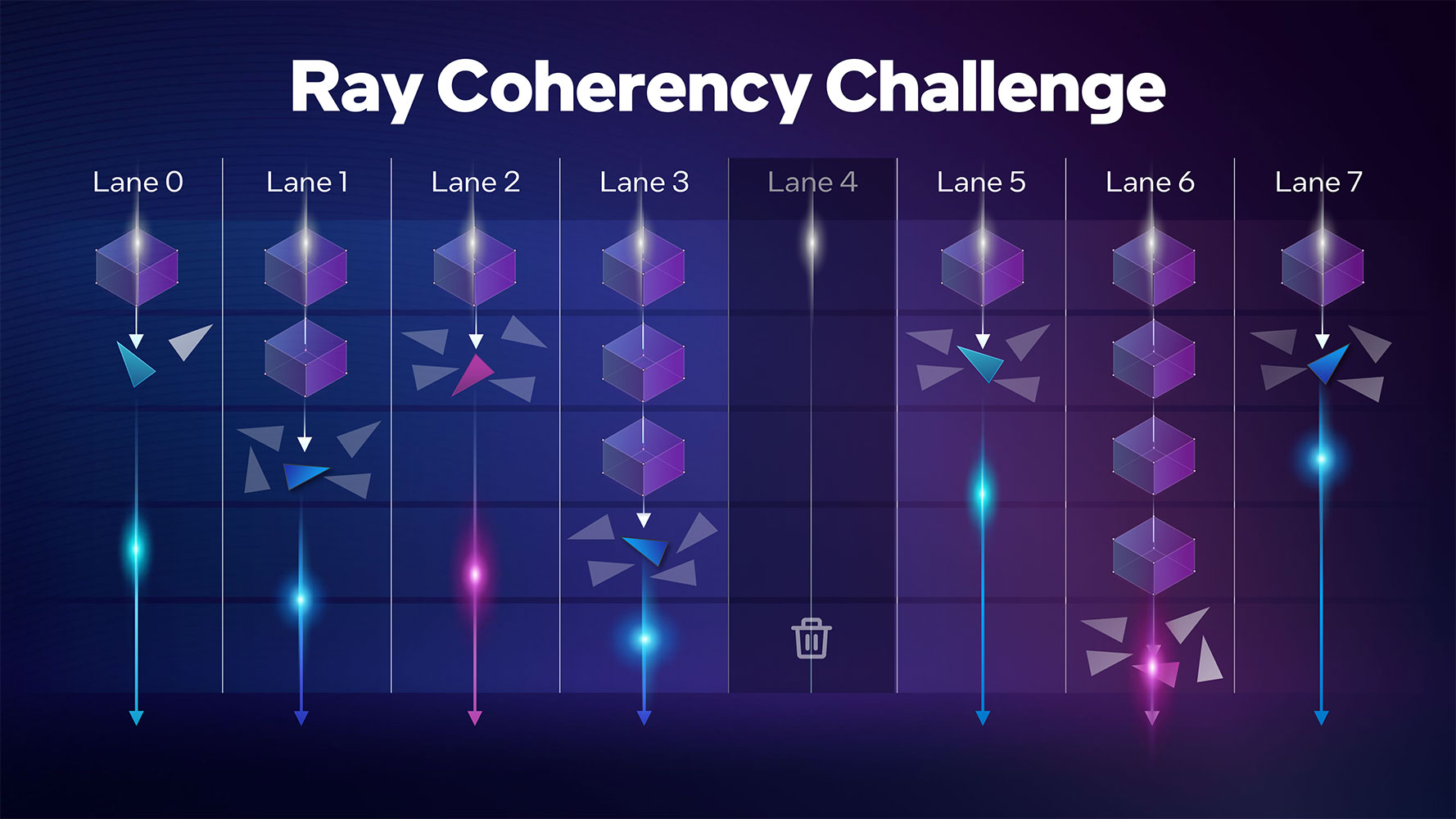
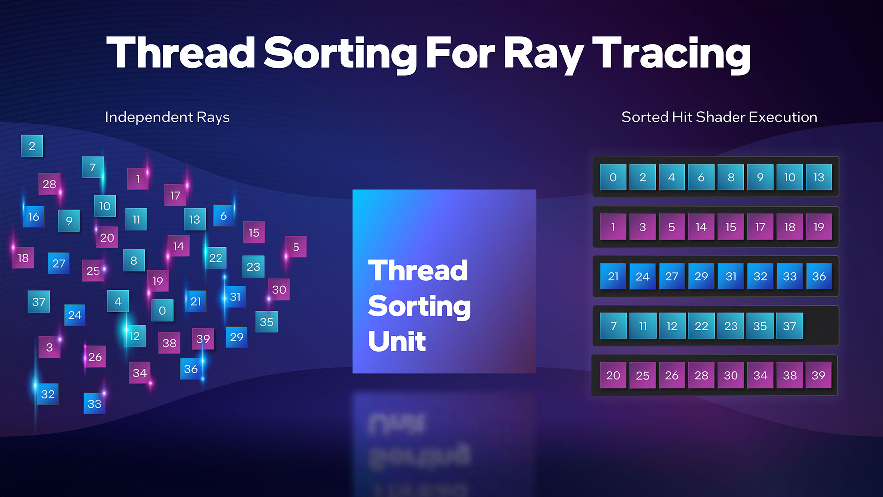
There are several optimizations that further reduce the burden of ray tracing operations on the main SIMD machinery, such as shader execution reordering which optimizes shader work threads for streamlined execution among the SIMD units. NVIDIA is only now implementing such a feature, with its GeForce "Ada" architecture. There's a special component in each Xe Core that reorders shader threads. It's essentially a very intelligent dispatch unit. Intel refers to its ray tracing architecture as Asynchronous.
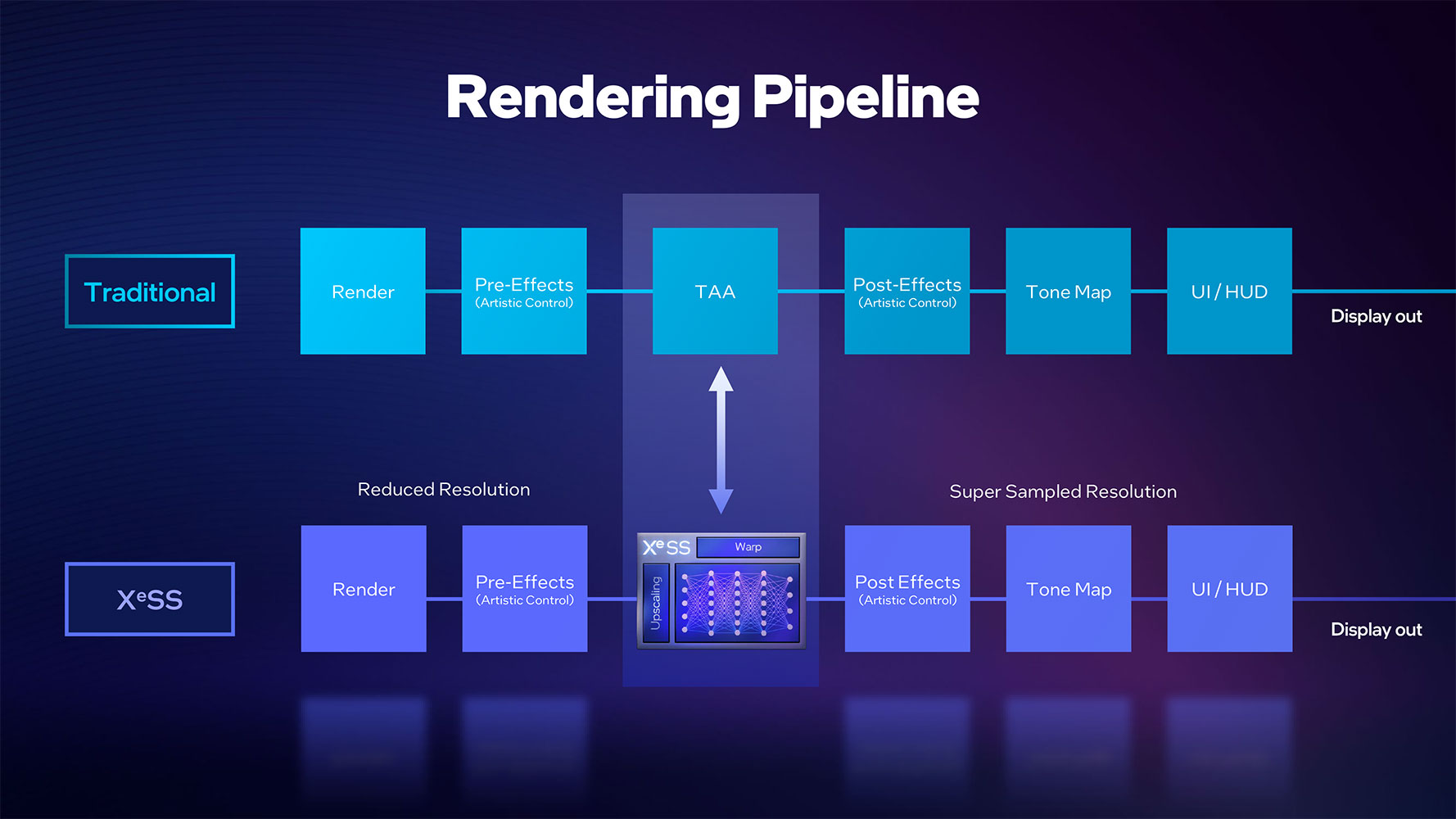
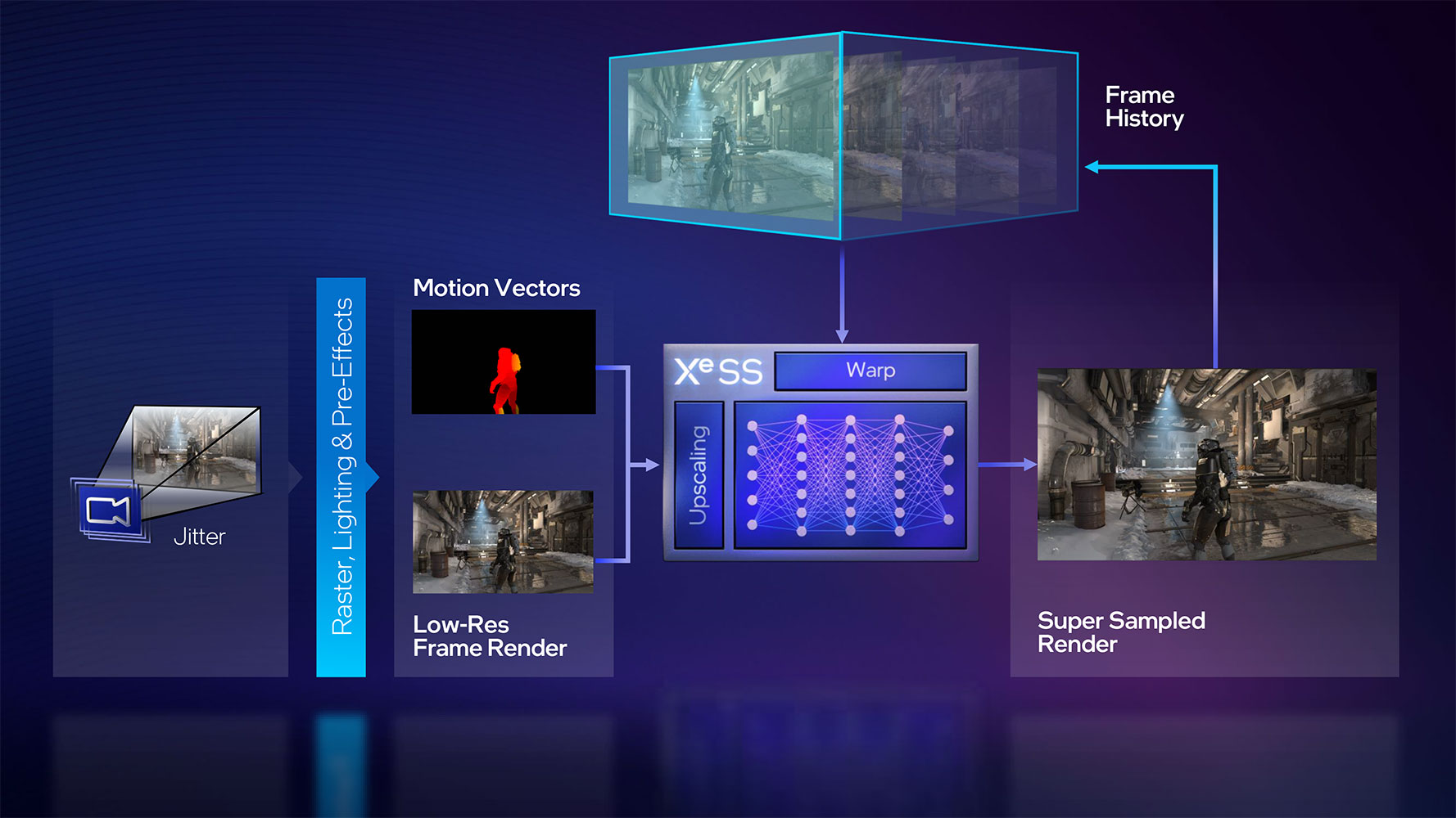
With Moore's Law tapering despite Intel claiming otherwise, the writing is on the wall—rendering at native resolution is over, at least in the performance and mainstream GPU segments. High-quality super resolution features such as DLSS and FSR are helping NVIDIA and AMD shore up performance at minimal quality loss, by rendering games at lower resolutions than native to the display; and upscaling them intelligently, with minimal quality losses. Intel's take is XeSS. The company claims that this is a 2nd generation super-res technology, on par with DLSS 2 and FSR 2.0. The XeSS upscaling tech is as easily integrated with a game engine's rendering pipeline as TAA (or AMD FSR). The XeSS algorithm is executed as XMX-optimized AI on Arc GPUs, and as DP4a-compatible code on other GPU brands. The algorithm takes into account low-resolution frame data, motion vectors, and temporal data from previously output high-res frames to reconstruct details, before passing on the high-res output to the game engine for post-processing and UI/HUD.
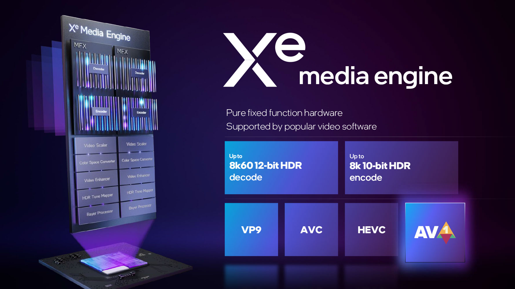
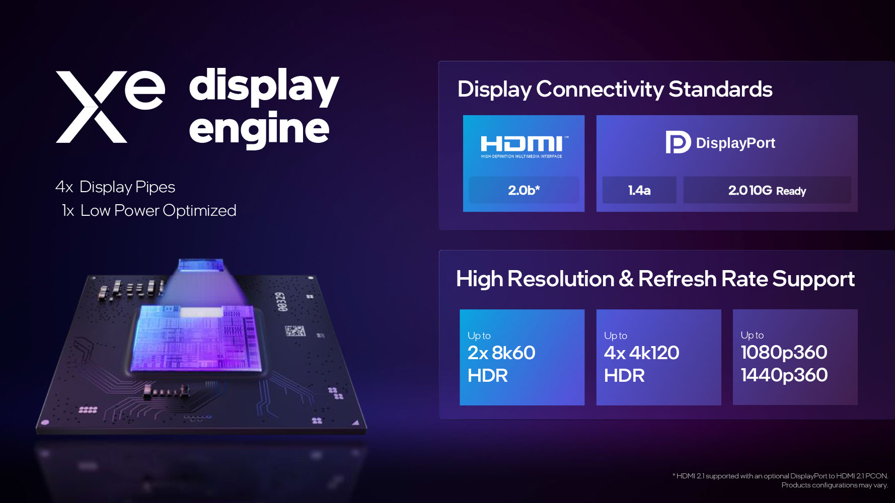
The Xe Display Engine is capable of up to two display outputs at 8K 60 Hz + HDR; up to four outputs at 4K 120 Hz + HDR, and up to four 1440p or 1080p with 360 Hz + HDR. VESA Adaptive Sync and Intel Smooth Sync features are supported. The latter is a feature that runs the GPU at its native frame-rate, while attempting to remove the screen-tearing from the display output. A typical Arc desktop graphics card has two each of DisplayPort 2.0 and HDMI 2.0b connections. The Xe Media Engine provides hardware-accelerated decoding and encoding of AV1, and accelerated decoding of H.265 HEVC, and H.264 AVC.
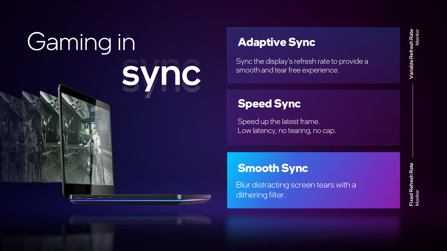

Besides VESA Adaptive Sync, the Xe Display Engine offers a software feature called Smooth Sync. This gives fixed refresh-rate monitors the ability to play games without V-Sync, rendering them at the highest possible FPS (and the least input latency), while attempting to eliminate the screen-tearing using a shader-based dithering filter pass. This is an extremely simply way to solve this problem, and we're surprised AMD and NVIDIA haven't tried it.
Packaging
The Card
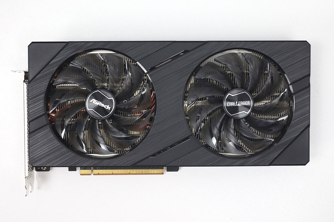
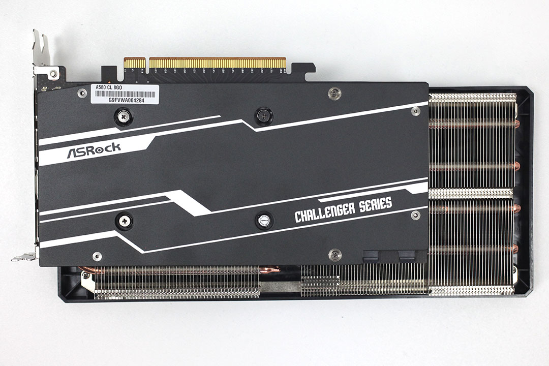
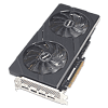
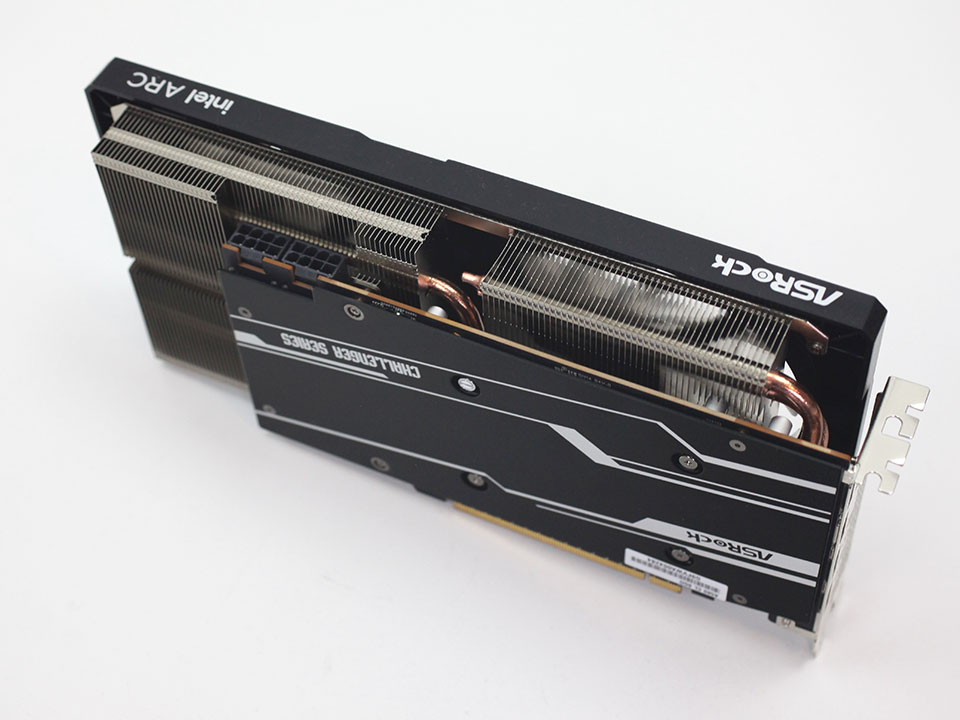
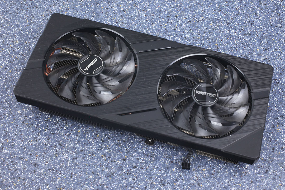
Despite Intel's blue color theme, ASRock is focusing on a clean, stylish experience with their card. The main color is black, with some highlights on the metal backplate.
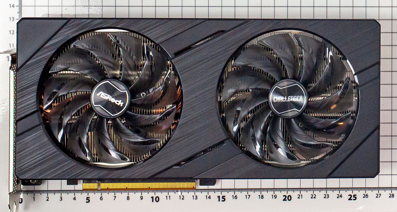
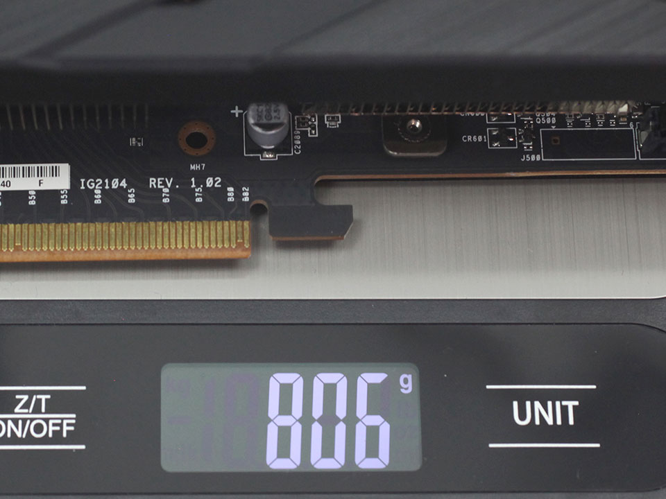
Dimensions of the card are 27.0 x 13.0 cm, and it weighs 806 g.
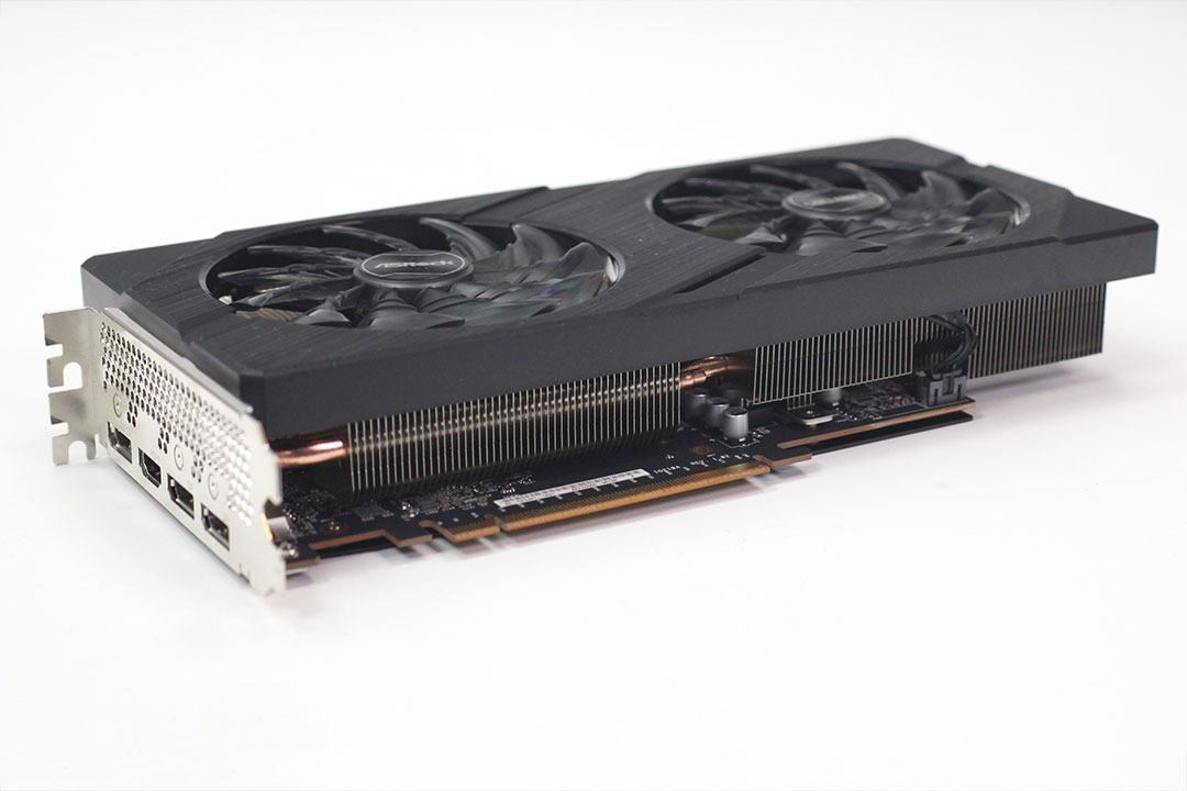
Installation requires three slots in your system. The card's width is 47 mm.
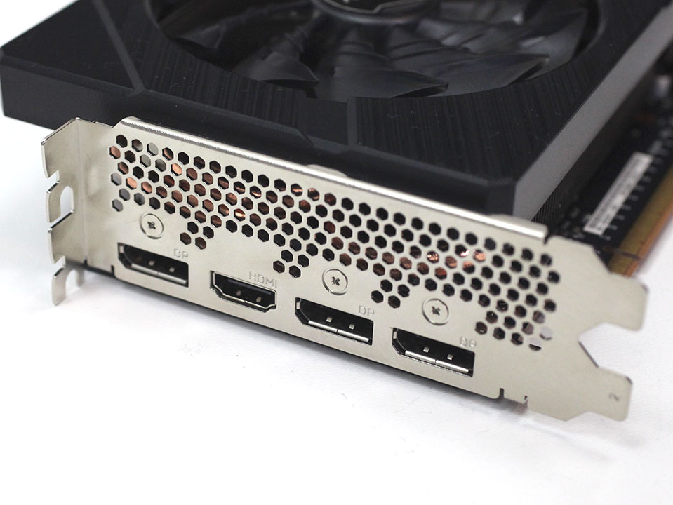
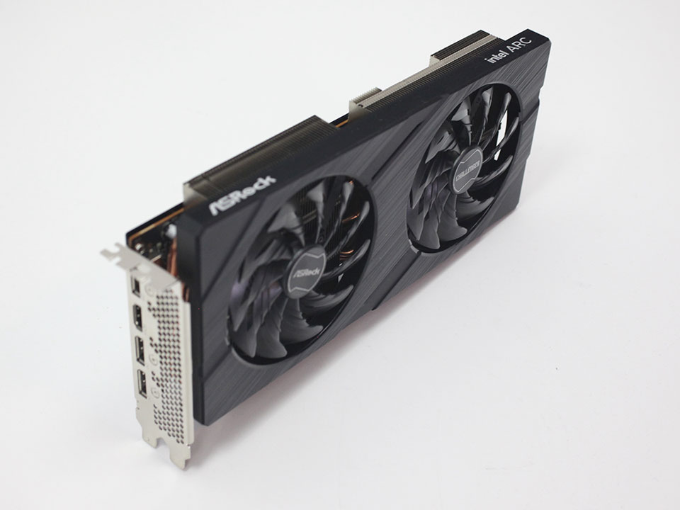
Display connectivity includes three standard DisplayPort 2.0 ports and one HDMI 2.0.
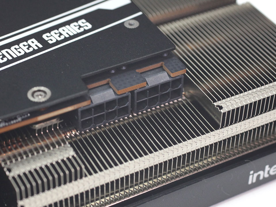
The card has two 8-pin power inputs. Combined with slot power, this allows a theoretical power delivery of up to 375 W.
Teardown
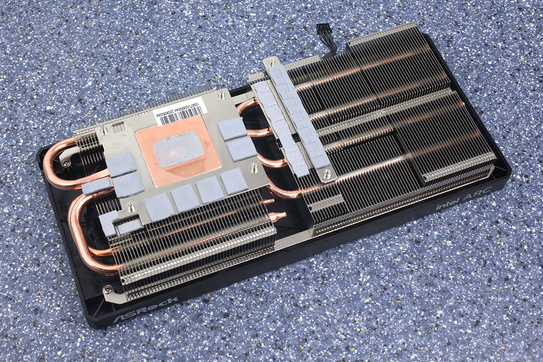
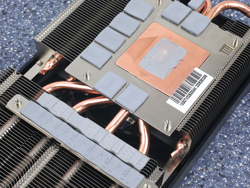
The main heatsink on the A580 uses four heatpipes and provides cooling for the GPU chip, the memory and the VRM circuitry.
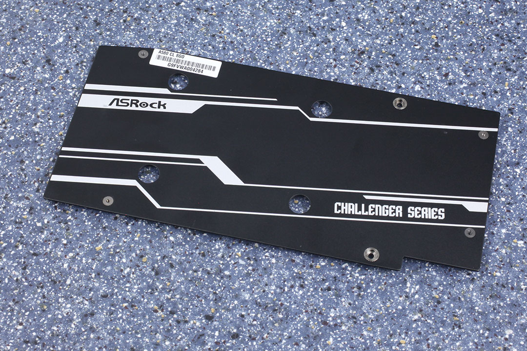
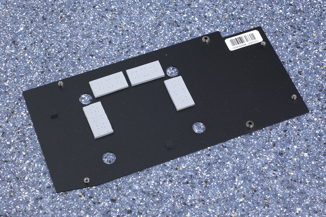
The backplate is made of metal and protects the card against damage during installation and handling.
High-resolution PCB Pictures
These pictures are for the convenience of volt modders and people who would like to see all the finer details on the PCB. Feel free to link back to us and use these in your articles, videos or forum posts.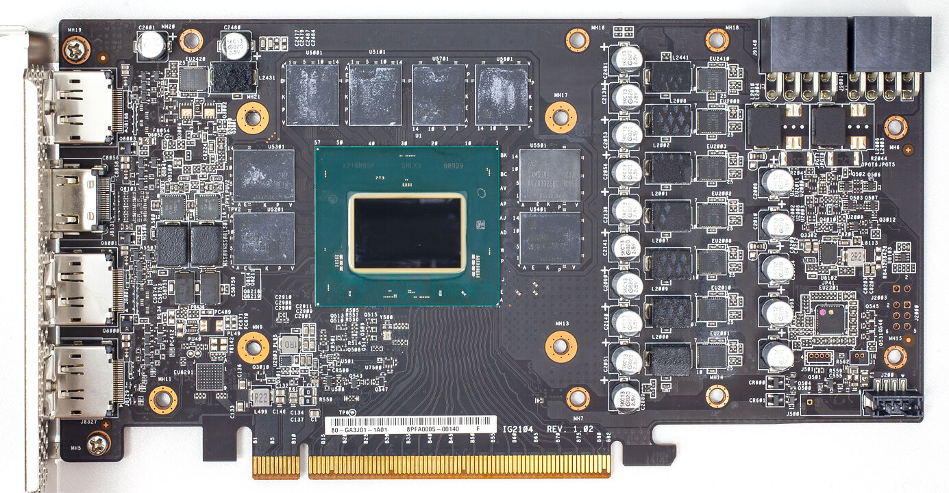

High-resolution versions are also available (front, back).
Our Patreon Silver Supporters can read articles in single-page format.
May 23rd, 2024 10:25 EDT
change timezone
Latest GPU Drivers
New Forum Posts
- Been away from PC gaming, a bit lost... (74)
- BSOD and Memory Errors (17)
- What's your latest tech purchase? (20645)
- Can anyone ID this fan? (prop only, no markings - super challenge!) (19)
- Removing the 12v sensing line on the thor 1200 (oringial) (13)
- What are you playing? (20740)
- Are all software/scheduling issues with e-cores fixed on Intel 12th to 14th Gen - Willing to give hybrid ach a chance now (105)
- FINAL FANTASY XIV: Dawntrail Official Benchmark (90)
- What phone you use as your daily driver? And, a discussion of them. (1521)
- Gigabyte am5 motherboard ddr5 not posting when rebooting (17)
Popular Reviews
- Ghost of Tsushima Performance Benchmark Review - 35 GPUs Tested
- Senua's Saga: Hellblade II Performance Benchmark Review
- Ghost of Tsushima: DLSS vs. FSR vs. XeSS Comparison Review
- CHERRY XTRFY M68 Pro Review
- PNY XLR8 Gaming EPIC-X RGB DDR5-6400 CL32 32 GB Review
- PMG Audio Apx In-Ear Monitors Review - $6500 Flagship!
- Upcoming Hardware Launches 2023 (Updated Feb 2024)
- TerraMaster D8 Hybrid Review
- Homeworld 3 Performance Benchmark Review - 35 GPUs Tested
- Quick Look: Huion Kamvas Pro 24 (4K) Graphics Tablet
Controversial News Posts
- Intel Statement on Stability Issues: "Motherboard Makers to Blame" (272)
- AMD to Redesign Ray Tracing Hardware on RDNA 4 (227)
- Windows 11 Now Officially Adware as Microsoft Embeds Ads in the Start Menu (173)
- NVIDIA to Only Launch the Flagship GeForce RTX 5090 in 2024, Rest of the Series in 2025 (154)
- AMD Hits Highest-Ever x86 CPU Market Share in Q1 2024 Across Desktop and Server (140)
- AMD RDNA 5 a "Clean Sheet" Graphics Architecture, RDNA 4 Merely Corrects a Bug Over RDNA 3 (139)
- AMD's RDNA 4 GPUs Could Stick with 18 Gbps GDDR6 Memory (114)
- AMD Ryzen 9 7900X3D Now at a Mouth-watering $329 (104)