 2
2
ASRock Radeon RX 7900 GRE Steel Legend Review
Pictures & Teardown »AMD RDNA 3 Graphics Architecture


The Radeon RX 7900 series debuts AMD's third generation RDNA graphics architecture, termed RDNA 3. With it, AMD plans to repeat the generational 50% performance/Watt gain it achieved with RDNA 2, which sprung it back to the high-end graphics segment after a long gap. AMD claims it succeeded in this endeavor, with a 54% generational performance/Watt gain. At the heart of this effort is the switch to the new TSMC 5 nm EUV foundry node. AMD figured out early on that it cannot build large monolithic GPUs on 5 nm without thinning its margins in the fight against NVIDIA, and set out to innovate the Chiplet architecture for the GPU. Under this, specific parts of the GPU that actually benefit from a switch to a newer foundry node, such as the Shader Engines, would be built on a centralized 5 nm die called the Graphics Compute Die (GCD), while those components that can make do with a less advanced node, namely the memory controllers and L3 cache, would be spun off to chiplets called Memory Cache Dies (MCDs), built on 6 nm.


The "Navi 31" GPU is hence a chiplet GPU and not a multi-chip module like "Vega 10." In a chiplet-based device, various components that can otherwise not exist on their own packages, are placed on a single package, with the goal of minimizing production costs, by stratifying their need for a new foundry node, such that only the most power-intensive IP receive the most advanced node. In a MCM, chips that can otherwise exist on their own package, are combined onto a single package for conserving PCB real-estate, or reducing latency. The GCD in the "Navi 31" GPU hence has all the shader engines, caches up to L2, the front-end Command Processor, Async Compute Engines (ACEs), the Display Engine, and the Media Engine. Each of the six MCDs has a 64-bit wide memory bus, and a 16 MB segment of the GPU's 96 MB Infinity Cache memory. The size of the Infinity Cache may have been generationally reduced (compared to 128 MB on "Navi 21"), but AMD has widened the memory bus itself, from 256-bit up to 384-bit.


Much of the architectural innovation is not with the chiplet design (a packaging innovation); but at the level of the RDNA 3 Dual-Compute Unit (or Compute Unit pair). The "Navi 31" GPU physically features 96 compute units spread across six Shader Engines. AMD claims that at the same engine clocks, the RDNA 3 CU offers a 17.4% IPC increase over the RDNA 2 CU. There are 20% more CUs over the "Navi 21," and these run at higher engine clocks, tapping into the power headroom afforded by the 5 nm process. These combined work out to the 54% generational performance uplift, with which AMD plans to retain competitiveness with NVIDIA's RTX 40-series "Ada" high-end SKUs.
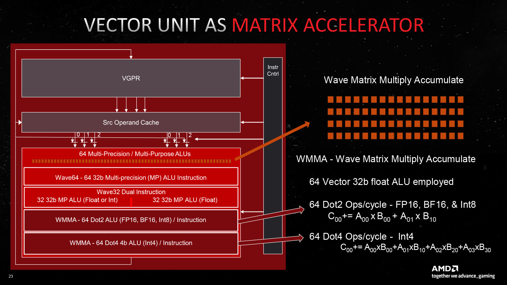

The new RDNA 3 CU introduces multi-precision capability for the 64 stream processors per CU: operating either as 1x SIMD64 or 2x SIMD32 units. The Vector Unit that houses these SIMD units can either function as a SIMD execution mechanism, or as a Matrix execution unit, thanks to the new AI Matrix Accelerator, which provides a 2.7x matrix multiplication performance uplift versus conventional SIMD execution. Also added are support for the Bfloat16 instruction-set, and SIMD8 execution. The GPU hence enjoys AI hardware-acceleration that can be leveraged in future feature-additions relevant to gamers, such as FSR 3.0. Game developers will also look for ways to exploit accelerated AI, now that all three brands feature it (NVIDIA Tensor cores and Intel XMX cores).


AMD's first-generation Ray Accelerator, introduced with the RDNA 2 architecture, was the result of a hasty effort to catch up to NVIDIA with a DirectX 12 Ultimate GPU, where they developed a fixed-function hardware to calculate ray intersections, and offloaded a large chunk of RT processing to the generationally-doubled SIMD resources. With RDNA 3, they've refined the Ray Accelerator to achieve an 80% ray tracing performance uplift over the previous generation, when you add up the Ray Accelerator count, their higher engine clocks, and other hardware-level optimizations, such as early subtree culling, specialized box sorting modes, and reduced traversal iterations.


There is a 50% ray intersection capacity improvement for the "Navi 31" GPU thanks to these optimizations, and cycles-per-ray reduction. Besides these, AMD has also made several improvements to the geometry- and pixel-pipes, with the introduction of the new multi-draw indirect accelerator (MDIA), which reduces CPU API and driver-level overheads by gathering and parsing of multi-draw command data. At the hardware-level 12 primitives per clock is now supported compared to 8 per clock on RDNA 2, thanks to culling. The core-configuration overall enables 50% more rasterized performance per clock.
The GCD features six Shader Engines, each with 16 compute units (or 8 dual compute units), which work out to 1,024 stream processors. Six such Shader Engines make up 6,144 stream processors with 96 Ray Accelerators and 96 AI Accelerators. The GPU has 384 TMUs, and a massive 192 ROPs—a 50% increase over "Navi 21." The Radeon RX 7900 XTX enables all 96 CUs, and maxes out the silicon, whereas the RX 7900 XT has 84 out of 96 CUs enabled, which work out to 5,376 stream processors, 84 Ray Accelerators, 336 TMUs, and an unchanged 192 ROPs. The new RX 7900 GRE has 80 CUs enabled, which work out to 5,120 stream processors, 80 Ray Accelerators, 320 TMUs, and 160 ROPs. The RX 7900 XTX gets 24 GB of GDDR6 memory across the GPU's entire 384-bit memory bus, with a memory speed of 20 Gbps (GDDR6-effective), which means 960 GB/s of memory bandwidth. The RX 7900 XT is equipped with 20 GB of memory across a narrower 320-bit memory bus carved out by disabling one of the six MCDs. At the same 20 Gbps speed, this yields 800 GB/s bandwidth. The RX 7900 GRE goes one further step down, with two of the six MCDs being disabled, for a 256-bit memory bus, running 16 GB of memory at 18 Gbps speed, for 576 GB/s of bandwidth.


AMD has significantly improved the Display Engine of "Navi 31" over the previous-generation in terms of connectivity. The new Radiance Display Engine comes with native support for DisplayPort 2.1, which enables 8K output at up to 165 Hz refresh-rate, or 4K at up to 480 Hz, with a single cable. AMD has refined its FSR 2 algorithm to support 8K (i.e. render at a lower resolution with FSR-enhanced upscaling), to make it possible to enjoy the latest AAA titles at playable frame-rates on 8K displays. All the RX 7900 series cards get two full-size DP 2.1 connectors, besides an HDMI 2.1b, and a USB-C with DP 1.2 passthrough. The "Navi 31" silicon receives full hardware-accelerated AV1 encode and decode capabilities, through dual independent encode/decoders, so two independent video streams can be simultaneously transcoded, or one stream at twice the framerate. With this generation, AMD is also introducing SmartAccess Video, a feature that lets the AMD driver leverage the hardware encoders of the RDNA 2 iGPU of Ryzen 7000 desktop processors, for additional encoding performance.
FidelityFX SuperResolution 3 Fluid Motion Frames (FSR 3 and FMF)

AMD announced the much awaited FidelityFX Super Resolution 3 and Fluid Motion Frames. FSR 3 is being announced as a technological rival to NVIDIA DLSS 3 Frame Generation. The premise with both technologies is the same—to effectively double frame-rates by generating alternate frames without running them through the entire graphics rendering pipeline, it's just that the two technologies differ in their approach to this goal.
FSR 3 builds on FSR 2 with its updated super resolution upscaler promising generational quality improvements at every given rendering resolution. Fluid Motion Frames (FMF) isn't the entirety of the FSR 3 feature-set, but is its most important feature-addition. FMF is a frame interpolation technology much like the one consumer televisions come with. Alternate frames are generated as an approximate of two frames. Where FMF differs from DLSS 3 Frame Generation is that while NVIDIA uses a hardware component called optical flow accelerator and the GPU's AI acceleration to generate an intermediate frame without involving the graphics rendering pipeline, FMF uses a certain amount of the graphics rendering pipeline. At a hardware level, FMF uses the main SIMD machinery of the GPU, leveraging asynchronous compute. As with DLSS 3 FG, FSR 3 FMF comes with added latency. NVIDIA counteracts this with Reflex, while AMD uses Radeon AntiLag+. Both technologies try to keep the frame queue short to reduce whole system latencies.
One major advantage FSR 3 FMF enjoys over DLSS 3 FG is that it works on any modern DirectX 12 GPU that supports async compute, since it doesn't require a specific hardware component the way DLSS 3 FG requires the Optical Flow Accelerator on NVIDIA "Ada" GPUs. The only limiting factor here is the performance. To be more specific, AMD says that all Radeon GPUs from RX 5700 series onward; and all GeForce GPUs from RTX 20-series onward, should support FSR 3 FMF. Also, FSR 3 FMF is as easy to integrate with games as FSR 2 is. The first games implementing FSR 3 FMF should arrive in Fall 2023. AMD is also working to extend FMF to Radeon Super Resolution, the driver-level technology that enables performance upscaling to even games that don't support FSR.
HYPR-RX

HYPR-RX is an interesting new feature in the AMD Software (control center) application. It is a one-click performance boosting technology that works with any DirectX 11 or DirectX 12 game. The software is a cocktail of Radeon Boost, Radeon AntiLag+, and Radeon Super Resolution, and applies the three features on any running game as needed, automatically. Radeon Boost improves performance by dynamically reducing the render resolution of a game when there's too much motion on the screen (and hence not enough detail needed). Radeon Super Resolution improves frame-rates as it applies FSR on the output of a game rendered at a lower resolution (including the frames lowered in resolution by Radeon Boost. AntiLag+ counteracts the latency added by these two, by shortening the frame queue. AFMF is part of the HYPR-RX feature-set, which can be activated with a single click.
May 9th, 2024 21:53 EDT
change timezone
Latest GPU Drivers
New Forum Posts
- AM5 boot times improve RADICALLY with memory context restore enabled (16)
- Graphics card running at 8x 4.0 not 16x 4.0 (2)
- Is hard drive sentinel trustworthy (6)
- dolby pro logic 2x settings menu in windows 10 (0)
- Dell Workstation Owners Club (3071)
- Only some humans can see refresh rates faster than others, I am one of those humans. (238)
- Soundblaster x-ae5 plus sometimes switches center channel to other channels. (2)
- not impressed - nvme vs ssd (76)
- Your way of cooling your PC? (100)
- Microsoft butchering Xbox Studios (42)
Popular Reviews
- CHERRY XTRFY M64 Pro Review
- Bykski CPU-XPR-C-I CPU Water Block Review - Amazing Value!
- Corsair iCUE Link RX120 RGB 120 mm Fan Review
- Corsair MP700 Pro SE 4 TB Review
- Upcoming Hardware Launches 2023 (Updated Feb 2024)
- Finalmouse UltralightX Review
- ThundeRobot ML903 NearLink Review
- AMD Ryzen 7 7800X3D Review - The Best Gaming CPU
- Sapphire Radeon RX 7700 XT Pure Review
- ASUS Radeon RX 7900 GRE TUF OC Review
Controversial News Posts
- Intel Statement on Stability Issues: "Motherboard Makers to Blame" (264)
- AMD to Redesign Ray Tracing Hardware on RDNA 4 (206)
- Windows 11 Now Officially Adware as Microsoft Embeds Ads in the Start Menu (169)
- NVIDIA to Only Launch the Flagship GeForce RTX 5090 in 2024, Rest of the Series in 2025 (144)
- Sony PlayStation 5 Pro Specifications Confirmed, Console Arrives Before Holidays (119)
- AMD's RDNA 4 GPUs Could Stick with 18 Gbps GDDR6 Memory (114)
- NVIDIA Points Intel Raptor Lake CPU Users to Get Help from Intel Amid System Instability Issues (106)
- AMD Ryzen 9 7900X3D Now at a Mouth-watering $329 (104)